India Unveils ‘Semicon 2.0’ to Accelerate Semiconductor Ecosystem
Ashwini Vaishnaw outlines six pillars covering chip design, semiconductor manufacturing, advanced packaging, R&D and talent development.
India is moving into the next phase of its semiconductor development with the launch of ‘Semicon 2.0’, a programme focused on expanding the country’s capabilities across chip design, manufacturing, advanced packaging, research and development, and talent development.
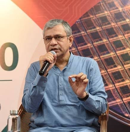
Speaking at SEMICON India 2026, Union Minister for Electronics and Information Technology Ashwini Vaishnaw said that Semicon 1.0 established the foundation for India’s semiconductor industry, while Semicon 2.0 will focus on expanding and strengthening the ecosystem built on that foundation.
According toAshwini Vaishnaw, Semicon 2.0 will be structured around six key pillars: design; machines and materials; semiconductor fabs; advanced packaging; research and development; and talent development.
Expanding India’s chip design ecosystem
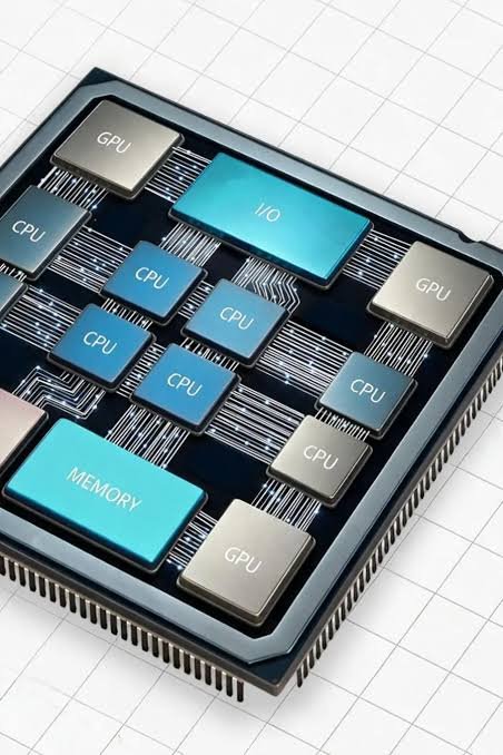
Under the design pillar, the government is targeting at least 200 startups and companies working on chip design across a range of semiconductor applications.
Ashwini Vaishnaw said that more than 105 startups had participated under Semicon 1.0, with around 20 receiving venture capital funding of approximately ₹800 crore.
The next phase is intended to further expand India's design capabilities and create a larger base of semiconductor companies developing products and solutions for different applications.
Building capabilities beyond semiconductor fabs
Ashwini Vaishnaw also highlighted the importance of developing the supporting infrastructure required for a complete semiconductor ecosystem.
Semicon 2.0 will therefore focus on capabilities spanning semiconductor equipment, materials, chemicals, gases and maintenance facilities. The government is seeking to develop these supporting industries alongside semiconductor fabrication, rather than concentrating solely on fabs.
This approach is intended to strengthen the broader supply chain required for semiconductor manufacturing in India.
Greater focus on manufacturing and advanced packaging
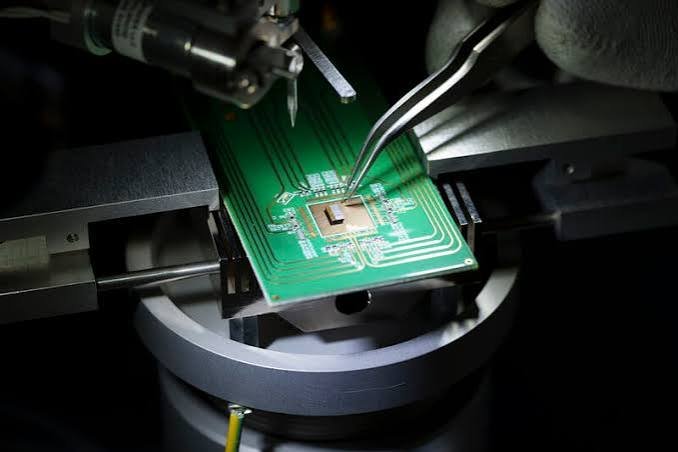
India also plans to expand its semiconductor manufacturing base through additional display, memory, silicon, compound and logic fabs, while increasing investment in advanced packaging.
Vaishnaw highlighted a 3D packaging facility being developed in Odisha as part of India's efforts to build capabilities in advanced semiconductor packaging.
The expansion of manufacturing and packaging capacity is expected to complement the country's growing semiconductor design ecosystem and strengthen capabilities across multiple stages of the value chain.
Industry-driven semiconductor R&D
Research and development will form another key pillar of Semicon 2.0.
According to Ashwini Vaishnaw, the government intends to encourage closer collaboration between industry and academia, with greater emphasis on applied and industry-driven semiconductor research.
The objective is to strengthen the connection between research capabilities and commercial semiconductor applications, while supporting the development of technologies relevant to industry requirements.
Developing semiconductor talent
Talent development will also receive greater attention under the new phase.
Ashwini Vaishnaw said India has already trained 70,000 design engineers in four years, compared with an original target of 85,000 over 10 years.
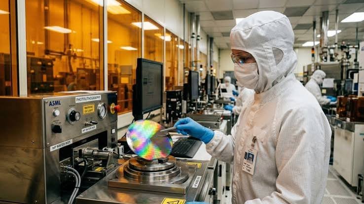
Under Semicon 2.0, the focus will expand beyond design engineers to include one lakh technicians and skilled workers for cleanrooms, semiconductor factories and production floors.
This expansion is aimed at creating the workforce required to support India's growing semiconductor manufacturing and production infrastructure.
Building on the foundation of Semicon 1.0
Ashwini Vaishnaw described India's semiconductor programme as a long-term journey, with Semicon 1.0 establishing the initial foundation and Semicon 2.0 focused on building a broader industry on that base.
The programme's six-pillar approach covers the semiconductor value chain from chip design and equipment to manufacturing, advanced packaging, research and development, and skilled manpower.
With the next phase, the government is seeking to expand India's semiconductor capabilities while developing the supporting ecosystem, talent base and industry-academia partnerships needed to sustain long-term growth.