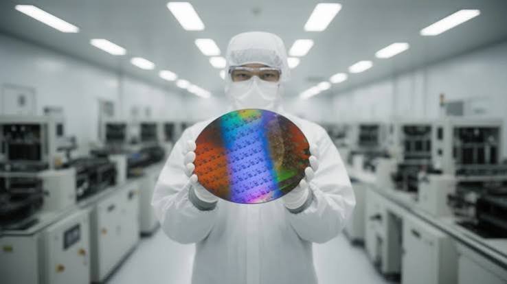
Lam Research and NY CREATES Launch Semiconductor Training Programme to Address US Talent Shortage
27 August 2026 |
Interaction
Five-year initiative will equip around 3,500 students with semiconductor process integration skills using Lam Research’s SEMulator3D virtual fabrication technology.
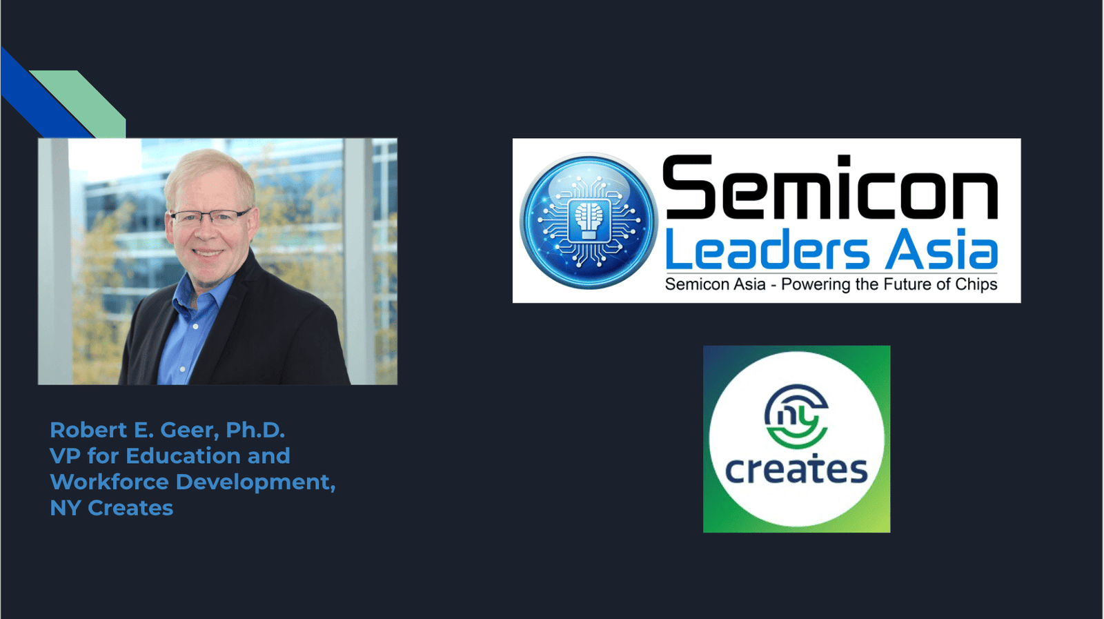
Robert E. Geer, Vice President for Education and Workforce Development at NY CREATES, speaks to Semicon Leaders Asia about the five-year partnership with Lam Research to strengthen semiconductor talent development. The programme aims to equip around 3,500 students with advanced process integration skills through virtual fabrication and digital-twin technology, helping prepare the workforce for the growing demands of the US semiconductor industry.
Q. What industry and workforce needs led Lam Research and NY Creates to launch this five-year semiconductor process integration training programme, and why is this collaboration important now?
There is unprecedented demand in New York State, and the U.S. overall, to grow our semiconductor industry. That growth starts with people. We need tens of thousands more engineers and technicians than we are able to produce. And those engineers need cutting-edge knowledge and skills in semiconductor processing. NY Creates’ partnership with Lam Research will bring their advanced technologies to training programs across New York.
Q. How does Lam’s SEMulator3D® virtual fabrication software differentiate the programme from traditional semiconductor manufacturing education?
Lam’s SEMulator3D platform gives students the ability to virtually construct the entire chip process flow. New courses and course modules will exploit this ability to give each student a ‘virtual fab’ to explore the impact of nanoscale design changes on chip performance.
Q. What specific process integration skills will students develop through SEMulator3D, and how closely are these skills aligned with the requirements of advanced semiconductor fabs?
In a fab the engineers who bring new materials or technologies into a given process flow are called ‘integrators.’ Integrators are a ‘jack of all trades’ in that they need to understand fabrication processes across the entire chip fabrication flow as opposed to a unit process engineer that focuses on a single process. As the complexity of chip fabrication increases, those integration skills become deeper and more complex. So, students need to understand much more about how process steps interact in terms of chip performance. With SEMulator3D, students will learn firsthand how changing the characteristics of one process step can change the overall device structure. These skills are invaluable in an advanced semiconductor fab.
Q. How will Lam Research and NY Creates measure the programme’s success in preparing approximately 3,500 students for careers in semiconductor manufacturing over the next five years?
The success of the program will be measured in part by the number of students introduced to SEMulator3D and in part by the number of course modules created or expanded using SEMulator3D. Long term, the success will be measured by the expanded abilities of learners to not only be familiar with prevailing IC process flows, but also through their ability to innovate using digital twin tools similar to SEMulator3D.
Q. What role do you see virtual fabrication playing in addressing the semiconductor industry's talent shortage, particularly when universities have limited access to expensive cleanroom facilities and manufacturing equipment?
Simulations and digital twins are not a complete substitute for working with physical systems. However, virtual fabrication is a powerful enabler for students. Students can innovate with entirely novel types of IC builds that otherwise could not be attempted if a hardware version were required. As importantly, the expectation is that digital twins will be a critical tool in a semiconductor technologist’s toolbox. Virtual fabrication like the kind enabled by SEMulator3D will see widespread adoption. So having students entering industry with an established expertise in these types of tools will be critical to address the workforce needs of the chip industry
Q. Looking beyond this initial programme, do Lam Research and NY Creates plan to expand the use of SEMulator3D into additional universities, technology nodes or areas such as advanced packaging and AI chip manufacturing?
The partnership between Lam Research and Creates is currently targeting a multi-university partnership for the expansion of SEMulator3D deployment in our region. The current focus of the simulation package is IC fabrication, and it is well-suited for simulating builds relevant to AI memory and logic. We are not currently evaluating its use for large-scale heterogeneous integration simulation (i.e. advanced packaging).