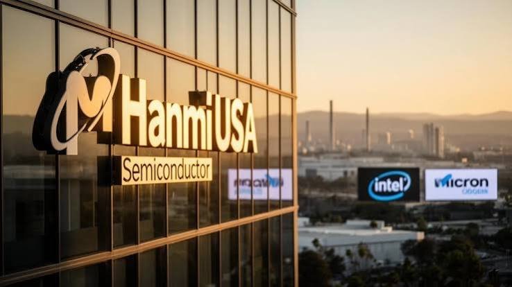
Hanmi Semiconductor Expands 2.5D Packaging Equipment Presence in Taiwan
Mass-production qualification at a Taiwanese foundry strengthens Hanmi’s position in advanced packaging as AI and high-performance computing drive demand for 2.5D technologies.
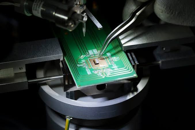
South Korean semiconductor equipment maker Hanmi Semiconductor has secured an important foothold in Taiwan’s advanced packaging market after its 2.5D bonding equipment passed mass-production qualification at a Taiwanese foundry. The company has subsequently begun supplying its packaging bonders to the unnamed customer, marking a significant step in Hanmi’s efforts to expand beyond its established high-bandwidth memory (HBM) equipment business.
The qualification is particularly significant because Taiwanese foundries have traditionally maintained strict equipment standards for mass-production lines. Hanmi’s successful entry provides the company with a reference customer as demand for advanced packaging equipment continues to rise alongside growing AI accelerator production.
Hanmi has been broadening its portfolio from HBM-focused bonding equipment towards 2.5D packaging technologies used for advanced AI and high-performance computing semiconductors. Its product range now includes flip-chip and thermocompression bonding equipment designed for different substrate sizes and packaging processes.
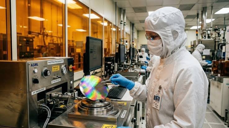
The company’s expansion comes as semiconductor manufacturers face increasing pressure on advanced packaging capacity. The rapid growth of AI accelerators is driving greater use of multi-die architectures, in which processors, accelerators and high-bandwidth memory are integrated within sophisticated packages. This is increasing demand for high-precision bonding equipment capable of handling increasingly complex packaging requirements.
Taiwan is becoming particularly important as foundries and outsourced semiconductor assembly and test (OSAT) providers expand their advanced packaging capacity. Foundries are not only increasing their own production lines but are also outsourcing selected packaging processes to companies such as ASE, SPIL and Amkor. As a result, demand for bonding equipment is spreading across a wider network of manufacturing sites rather than being concentrated solely within foundry-owned facilities.
Hanmi’s move into the Taiwanese market therefore represents more than a single equipment supply agreement. It demonstrates the company’s efforts to establish its 2.5D packaging technology within one of the world’s most important semiconductor manufacturing ecosystems. The qualification could also provide a foundation for further customer expansion as AI-driven packaging demand continues to grow.
The company is simultaneously increasing its global manufacturing and market presence. Hanmi announced plans in August to acquire a manufacturing facility in Incheon, South Korea, for approximately US$91.4 million, supporting additional bonding-equipment production capacity amid strong demand from the AI semiconductor market.
However, Hanmi still faces strong competition in the global bonding equipment market from established suppliers including ASMPT, BESI and Kulicke & Soffa. Expanding its customer base after securing mass-production qualification in Taiwan will therefore be an important next step in determining how successfully the company can translate its HBM expertise into a broader advanced-packaging business.
Hanmi’s progress also reflects a wider shift in the semiconductor equipment industry. As AI and high-performance computing drive increasingly complex chip architectures, advanced packaging is becoming a critical part of overall semiconductor performance. For equipment suppliers, establishing early positions in 2.5D and other advanced packaging processes could become increasingly important as foundries and OSAT providers scale capacity to meet the next generation of AI chip demand.