RAAAM Memory Technologies Targets SRAM Scaling Challenges with GCRAM
13 November 2026 |
Interaction
GCRAM technology aims to improve on-chip memory density, reduce power consumption and support next-generation AI processors, as RAAAM expands its US semiconductor partnerships.
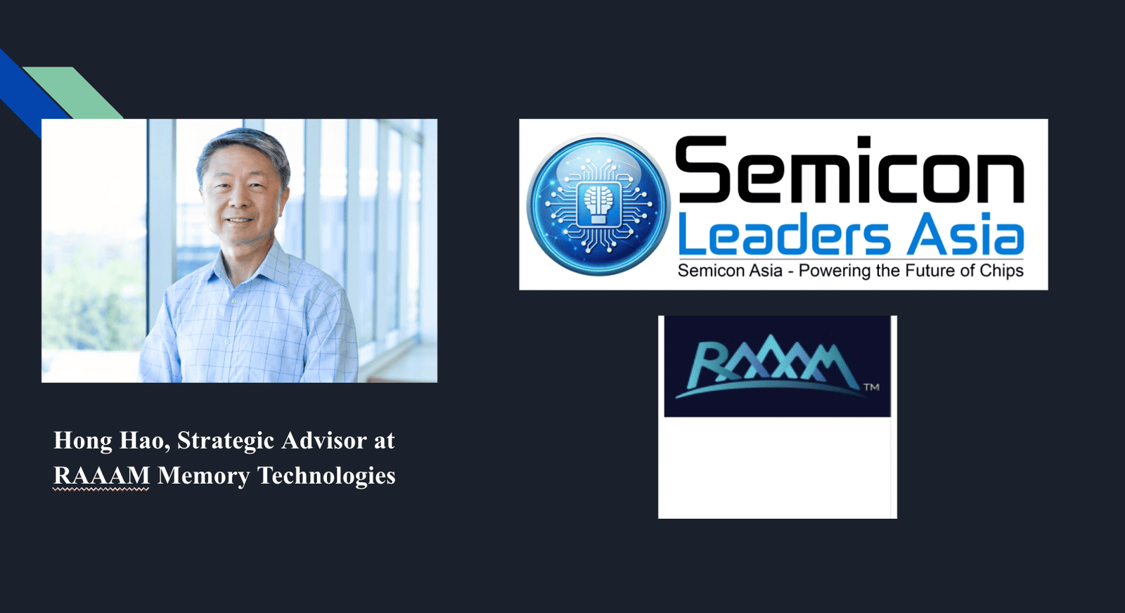
As AI chips demand greater memory capacity, SRAM scaling is becoming a major challenge for semiconductor manufacturers. RAAAM Memory Technologies aims to address this through its GCRAM technology, designed to reduce chip area and power consumption.Semicon Leaders Asia speaks with Hong Hao, Strategic Advisor at RAAAM Memory Technologies, about GCRAM’s commercial potential, CMOS compatibility and plans to strengthen semiconductor partnerships in the United States.
Q. RAAAM Memory Technologies has appointed you as Strategic Advisor. What attracted you to the company, and what will be your main priorities in this new role?
The semiconductor industry has had to manage the SRAM scaling challenges in the most advanced process technology nodes. On the one hand, more applications are demanding more and more on-die SRAM. On the other hand, SRAM size scaling has dramatically slowed in the most advanced technology nodes, leading to both size and power inefficiencies. These two factors combined have elevated SRAM to one of the key challenges in continuing to deliver the benefits of most advanced nodes in real products. So, when I was introduced to RAAAM and dug deeper into the GCRAM technology, I immediately became attracted to the potential of GCRAM as a game changing solution to the SRAM scaling challenge. The timing couldn't have been better - GCRAM arrives at this pivotal time when the AI buildout demands enormous amount of silicon and GCRAM's benefits can be appreciated in wide ranging products.
Q. You bring more than 30 years of experience from companies including Intel Foundry and Samsung Electronics. How will your experience help RAAAM strengthen its relationships with semiconductor companies and foundry partners?
I have had long experience in foundry business strategy, business development and customer engagement, covering broad based customer tiers and applications. RAAAM's GCRAM technology and solutions target essentially the same chip design customers a foundry does. So I can draw on these experiences to advise RAAAM on go-to-market strategies, customer engagement strategies, and ecosystem strategies. My numerous connections in the industry can help RAAAM open the right doors to customers. My experience competing and winning customers as "underdogs" also can be valuable to RAAAM as a new industry entrant.
Q. RAAAM’s GCRAM technology aims to address the growing limitations of SRAM in modern chip designs. What are the main advantages of GCRAM, and how could it benefit chipmakers in terms of performance, power consumption and cost?
GDRAM directly addresses the most critical SRAM challenges: die area and power consumption. Die size reduction directly translates to cost reduction as a result of smaller die size and higher yield for the same memory capacity. Designers could also expand on-die memory capacity without increasing die size, leading to improved system performance. Reduction in power consumption directly impacts overall chip and system level power consumption and leads to total power and cooling infrastructure simplification and cost reduction. GCRAM benefits are easy for chip architects and designers to understand. The key is to demonstrate real silicon validation and qualification to ensure these GCRAM can be manufactured in high volume just like SRAM.
Q. As AI and high-performance computing continue to drive demand for more memory on chips, how are customer requirements changing, and where do you see the biggest market opportunities for RAAAM?
AI and high performance computing demands more on-die SRAM. I see AI and high performance computing and networking in general as a very large and immediate market opportunity. However, GCRAM can also benefit other high volume applications equally, including mobile, personal computing, automotive, etc.
Q. One of RAAAM’s key advantages is that its memory technology can be manufactured using standard CMOS processes. How important is this compatibility for foundries and chip designers, and how could it help speed up commercial adoption?
The ability to manufacture GCRAM using standard CMOS logic process is a huge differentiation from all previous attempts to replace on-die SRAM. Foundries develop, qualify, and run enormous volume on standard logic processes for all kinds of products. Any deviation from standard logic processes would require a foundry to have custom process steps that need extra time and resources to develop and may not benefit from the high operational efficiency and yield enjoyed by standard processes. Depending on what extra or different steps are required, the normally well established IP and EDA ecosystem for a standard process may need to be customized and this can be highly costly or simply not feasible. So any solution that requires special process steps is bound to have limited success, whereas a solution that fits seamlessly in standard processes can be adopted without any issue by all designs.
Q. RAAAM is looking to expand its presence and customer relationships in the United States. What are the next steps in this expansion, and how do you plan to help the company build partnerships and bring GCRAM technology to more semiconductor customers?
The US is the largest market for semiconductor product designs. So it is naturally very critical for RAAAM to target the US market as the highest priority. As a new entrant, it is critical for RAAAM to identify and prioritize target market segments, and then focus on winning "anchor" customers that are leaders in each of the target segments. Winning "anchor" customers would not only provide business scale by virtue of their typical size, but also lead to credibility for other target customers in the same or adjacent segments. I plan to help RAAAM in the whole lifecycle of market segmentation and prioritization, customer engagement strategy and silicon data preparation, customer introductions and engagement, and deal structures and commercial terms.