SUSS Expands into Wafer Cleaning with GreenTec Solutions and 2027 Manufacturing Roadmap
22 October 2026 |
Interaction
The GT200 platform targets 200 mm MEMS, RF and power semiconductor applications, with high-volume manufacturing equipment planned for 300 mm wafers in 2027 and 200 mm wafers in 2028.
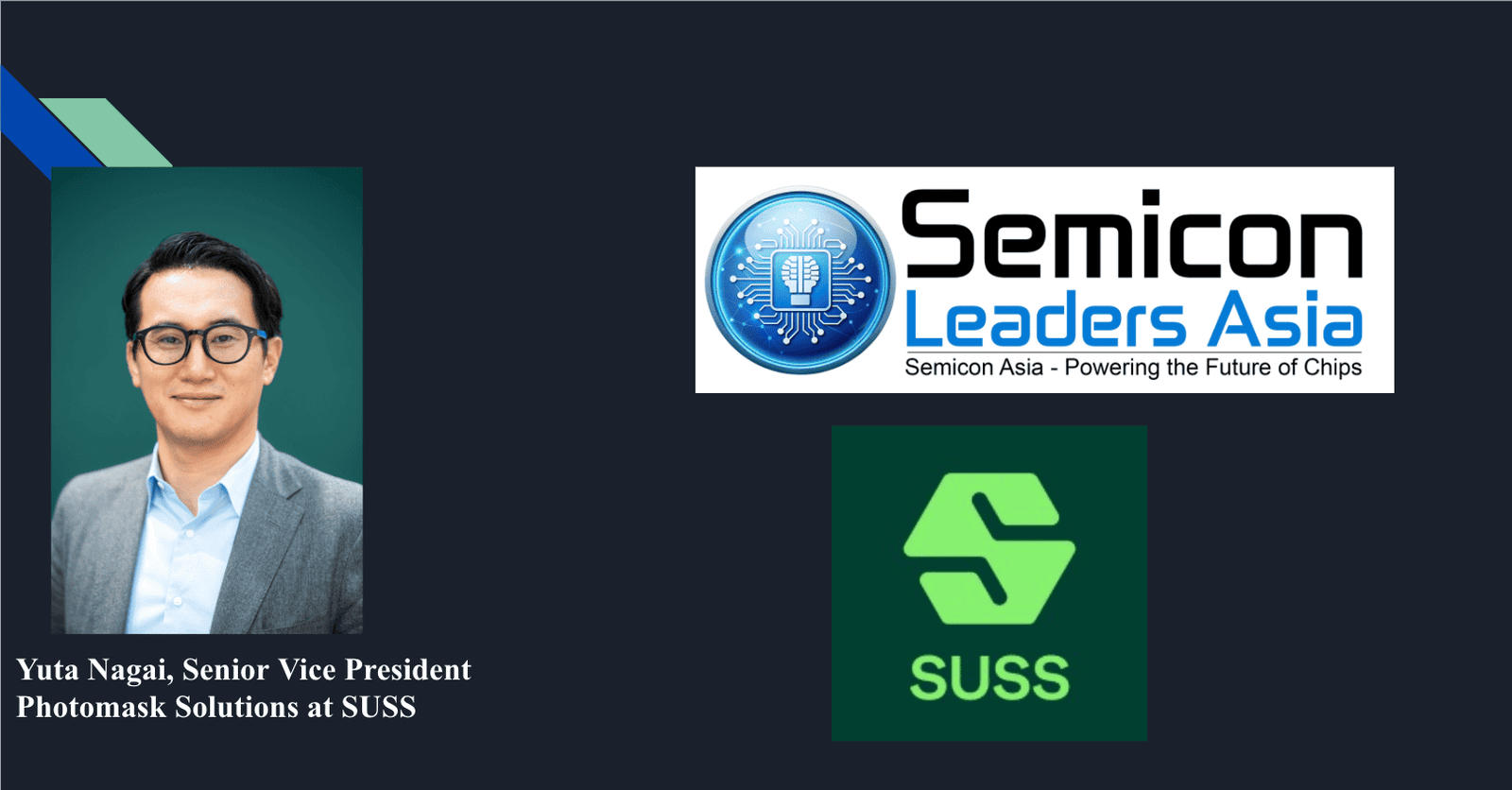
As advanced packaging and semiconductor manufacturing become increasingly complex, demand for efficient, sustainable wafer-cleaning technologies is growing. SUSS is entering this market with GreenTec Solutions, expanding its photomask cleaning expertise into wafer-level applications. Semicon Leaders Asia speaks with Yuta Nagai, Senior Vice President, Photomask Solutions at SUSS, about the company's growth strategy, GreenTec technologies, customer adoption and opportunities across the global semiconductor industry.
Q. What prompted SUSS to enter the wafer-level cleaning market at this stage, and how does the launch of GreenTec Solutions fit into the company’s Ambition 2030 growth strategy?
The semiconductor industry is undergoing a fundamental transformation. As conventional device scaling becomes increasingly challenging, advanced packaging, heterogeneous integration and 3D stacking are becoming essential approaches to improving semiconductor performance. Consequently, the traditional boundaries between front-end and back-end manufacturing are becoming less distinct, creating new requirements for advanced process control and cleaning technologies.SUSS has spent decades developing highly specialized cleaning technologies for photomask applications, where even the smallest particles or surface damage can have significant consequences. Defects on a photomask can be repeatedly transferred during lithography, while the high value of these masks makes preserving their integrity and extending their lifetime critically important.
To address these challenges, we have developed innovative cleaning technologies that reduce reliance on aggressive chemicals, establishing SUSS as a technology leader in photomask cleaning.
With the ongoing transformation of semiconductor manufacturing, we have received increasing interest from customers in applying these capabilities to wafer-level processes. In particular, the potential to address contamination challenges that conventional cleaning methods struggle to resolve has attracted considerable attention.
Take for example photoresist removal after plating in wafer-level packaging. Thick resist is typically removed with a long solvent soak followed by a single-wafer finish, often using solvent and hydroxide chemistries that require careful handling, abatement and disposal. Our customers asked whether the approach we use on photomasks could do this with water as the main medium.
Our decision to enter the wafer cleaning market is therefore not simply driven by the size of the market opportunity. It is driven by the convergence of changing industry requirements, customer demand and our unique technological capabilities. GreenTec represents the next step in transforming these capabilities into a new product portfolio and expanding our addressable market.This is closely aligned with Ambition 2030: leveraging our established technological leadership to enter adjacent markets, create new business opportunities and build sustainable engines for future growth.
Q. With advanced packaging, heterogeneous integration, AI and high-performance computing driving demand for wafer-cleaning equipment, which applications and market segments offer the strongest growth opportunities for SUSS?
Advanced packaging, heterogeneous integration, AI and high-performance computing are already important growth drivers for SUSS. Through our established coating, projection lithography, and bonding equipment portfolio, we actively support customers in these rapidly evolving areas.
For GreenTec, however, we are taking a deliberate, step-by-step approach to market entry. Rather than immediately targeting the highly competitive 300 mm market, where many of these advanced applications are concentrated, we intend to first establish our technological capabilities and customer references in the 200 mm segment.We see growing opportunities in 200 mm applications such as MEMS, RF, power semiconductors and selected CMOS processes. These markets are experiencing increasing process complexity and evolving cleaning requirements, creating opportunities for differentiated solutions.
Our strategy is to build practical application experience, demonstrate process performance and establish customer confidence in the 200 mm market before progressively expanding into 300 mm manufacturing.By following this approach, we aim to enter the larger advanced semiconductor manufacturing market with proven technologies, established process know-how and a solid foundation for sustainable growth.
Q. GreenTec Solutions brings SUSS’ established TurbulenStrip and CrustBuster technologies from photomask processing into wafer-level manufacturing. What advantages does this approach offer customers, particularly in terms of cleaning performance, chemical consumption and overall cost of ownership?
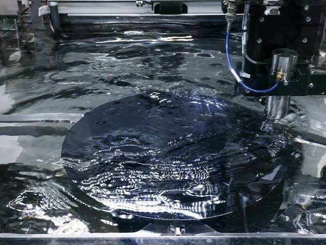
Our approach combines different cleaning technologies to address the increasingly diverse requirements of semiconductor manufacturing, rather than relying on a single cleaning mechanism.CrustBuster builds on our experience in photomask processing and is designed to remove photoresist and organic materials using water as the primary cleaning medium. This approach offers the potential to minimize the impact on underlying films and sensitive substrate structures, while reducing dependence on aggressive chemicals. TurbulenStrip, on the other hand, is a newly developed green cleaning technology for wafer applications, created in collaboration with a chemical industry partner. It is designed to handle a wide variety of surface conditions and multilayer structures while maintaining high throughput. Following the removal process, our final rinse unit incorporates advanced physical cleaning technologies developed through our photomask expertise. These technologies are designed to maximize particle removal efficiency while minimizing mechanical damage to sensitive surfaces.
Cost of ownership in cleaning is much more than the tool price - chemical purchase, storage, exhaust and abatement, waste treatment, EHS (Environment, Health and Safety) compliance, cycle time and rework all add up. Water-based processing reduces several of these at the same time, and combining batch and single-wafer steps in one hybrid design lets customers match the process to the layer instead of the other way round.
The key advantage is the ability to combine complementary cleaning mechanisms and optimize the overall process for different substrate and material conditions.
Conventional cleaning approaches often depend heavily on a single mechanism, which can limit process flexibility and make optimization challenging when substrate conditions vary.By integrating these technologies, we aim to provide a wider process window, improved process stability and greater flexibility across different applications.At the same time, reduced chemical consumption, improved throughput and more efficient process integration have the potential to contribute to a competitive total cost of ownership.Ultimately, our objective is to provide customers with both greater process flexibility and stronger manufacturing economics.
Q. The GT200 initially targets 200 mm applications, including MEMS, RF, power devices and CMOS. Which of these segments do you expect to see the earliest customer adoption, and what feedback have you received from potential customers so far?
These application segments are characterized by mature manufacturing technologies and well-established production processes. However, maturity does not necessarily mean that existing processes can remain unchanged. Increasing diversity in substrate materials, more complex device structures and evolving environmental regulations, particularly those affecting chemical usage, are creating a growing need to reconsider conventional cleaning approaches. Introducing new cleaning technologies into established manufacturing environments requires more than simply replacing one piece of equipment with another. Customers need a technology partner with broad application knowledge, process flexibility and the ability to support a controlled transition without compromising manufacturing performance. This is where we believe SUSS can provide significant value.
Our experience across different semiconductor manufacturing applications, combined with GreenTec's complementary cleaning technologies, enables us to offer flexible solutions tailored to a wide range of substrate and process requirements.
Initial customer discussions indicate interest in solutions that can address new material and cleaning challenges while reducing chemical dependency.
Regulation is moving in the same direction. In the European Union, the solvent NMP has been under strict worker-exposure limits since 2020, and two of its common substitutes, DMAC and NEP, come under the same kind of limits from December 2026. Fabs that change chemistry now want to change it once.
Rather than predicting that one specific segment will adopt our technology first, we are focusing on applications where changing process requirements create the strongest need for a new approach. We believe these opportunities will provide the foundation for early customer adoption and long-term partnerships.
Q. SUSS has brought forward its plans to introduce a 300 mm high-volume manufacturing platform in 2027, followed by a 200 mm HVM platform in 2028. What customer requirements are driving this accelerated roadmap, and how do you plan to support customers moving from process qualification to volume production?
Our internal evaluations have demonstrated that the GT200 is capable of supporting not only research and development activities but also early production applications.This is an important milestone because it allows us to move beyond laboratory-level technology demonstrations and begin validating our solutions under practical manufacturing conditions.Our immediate priority is to accelerate field evaluations with selected customer partners who are willing to work closely with us on process qualification and early production implementation. At the same time, we see significant opportunities to shorten the development cycle of our next-generation platforms by transferring the application knowledge, process experience and technological capabilities established in the 200 mm environment to our future 300 mm solutions. In parallel, we are working to optimize our supply chain and equipment architecture to support scalable manufacturing and more cost-effective solutions.
Our accelerated roadmap is therefore built around two parallel priorities: validating our technology with customers as early as possible and industrializing our platforms efficiently for high-volume manufacturing.
The GT200 provides the initial qualification and early production foundation, while our planned 300 mm HVM platform in 2027 and 200 mm HVM platform in 2028 will support the transition toward larger-scale manufacturing.
By working closely with customers throughout this process, we aim to reduce qualification risks, accelerate technology adoption and provide a clear pathway from initial evaluation to volume production.
Customers can already run their own wafers at our application center in Sternenfels. We measure what matters to them on their own structures - residue removal, damage and metal loss, cycle time, and chemistry, water and energy per wafer. That data, not a datasheet, is the basis for a field evaluation and later volume production.
Q. The wafer-cleaning market represents an estimated €5.4 billion opportunity, but it also has established equipment suppliers. How does SUSS plan to position GreenTec Solutions against existing solutions, and what role do you expect this business to play in the company’s future revenue growth?
We have no intention of competing with established equipment suppliers across every application or market segment. Our objective is not simply to introduce another cleaning tool into an already competitive market. Instead, we want to become a technology and solution partner for customers developing their next generation of semiconductor manufacturing processes. We believe our strongest opportunities will emerge where conventional cleaning approaches face technical limitations, where new materials and substrate structures require greater process flexibility, or where customers are looking for more sustainable and economically attractive alternatives. In these areas, our combination of specialized cleaning technologies, broad application knowledge and close customer collaboration can create meaningful differentiation.
Our ambition is to become a partner that helps customers realize their future manufacturing roadmaps and accelerate their own business development.
We believe sustainable revenue growth will follow once we have established technological credibility, demonstrated measurable customer value and gained recognition as a trusted solution provider. Looking ahead, we see the potential for GreenTec to develop into a business generating more than a few hundred million euros in annual revenue over the longer term. However, our immediate focus is not on maximizing short-term sales. It is on building the technological foundation, customer partnerships and execution capabilities necessary to achieve that ambition. For us, success means creating a sustainable, scalable business that contributes meaningfully to SUSS' long-term growth while helping our customers address the next generation of semiconductor manufacturing challenges.
Our message to the industry is simple: “Bring us your hardest cleaning step. If we cannot show a measurable improvement on your wafer, in cost, performance or chemistry, we have not earned the tool.”