The AI Chip Supply Chain in 2026: 10 Pinch Points, Ranked by How Long They Will Last
HBM, advanced packaging and leading-edge wafers are tight today, but they are not equally durable constraints. Some should loosen as 2027 capacity arrives. Others, from substrates and power delivery to cleanrooms and skilled labour, will follow the AI build-out well beyond the next product cycle.
SEMICON LEADERS ASIA ANALYSIS | OCTOBER 2026
Key takeaways
- HBM is the most severe shortage of 2026, but not the most durable. Record memory capex should bring meaningful relief by 2028, even if supply does not fully normalise in 2027.
- Wafers, CoWoS-class packaging and liquid cooling are cyclical constraints. Committed capacity with visible start dates should ease them from the second half of 2027.
- Substrates, photonics, power, cleanrooms and people are structural constraints. They depend on new materials, new architectures, construction timelines or training pipelines that money alone cannot compress.
- Procurement and investment strategies should split along the same line. Short-term premiums suit cyclical shortages. Structural ones call for second sources, long-term agreements, co-investment and design changes.
The most useful question about the AI semiconductor supply chain in late 2026 is no longer simply: what is in shortage?
Almost everything around a high-end accelerator is under some form of pressure. Leading-edge logic, high-bandwidth memory, the interposers and substrates that tie them together, the test cells that verify them, the optics that connect them and the power and cooling that keep them running are all being stretched at the same time. Ask a procurement head at a hyperscaler, a server maker or an AI start-up what is hard to get, and the honest answer is most of the bill of materials.
The scale of the response is unprecedented. TSMC says the gap between demand and supply remains large even as it runs a 2026 capital budget of US$60 billion to US$64 billion and builds 13 leading-edge and advanced-packaging fabs in Taiwan, plus another five to six overseas. SEMI now expects global 300mm front-end fab equipment spending to reach US$149 billion in 2026, up 31% year on year, and to keep rising at double-digit rates through 2029.
ASE is seeing the same pressure further down the chain. In its second-quarter materials, the company described hardware infrastructure as a bottleneck spanning capacity, automation and innovation. Its second-quarter equipment spending included US$840 million for packaging and US$804 million for testing, and management raised planned investment because near-term growth was being limited by how quickly equipment and facilities could be installed.
But these constraints will not clear together.
Some have visible capacity arriving in 2027. Others require new cleanrooms, new materials, different architectures or thousands of experienced engineers. That distinction matters to buyers deciding what capacity to reserve, to investors deciding which suppliers have pricing power that can survive the next twelve months, and to governments across Asia deciding where industrial policy money will actually move the needle.
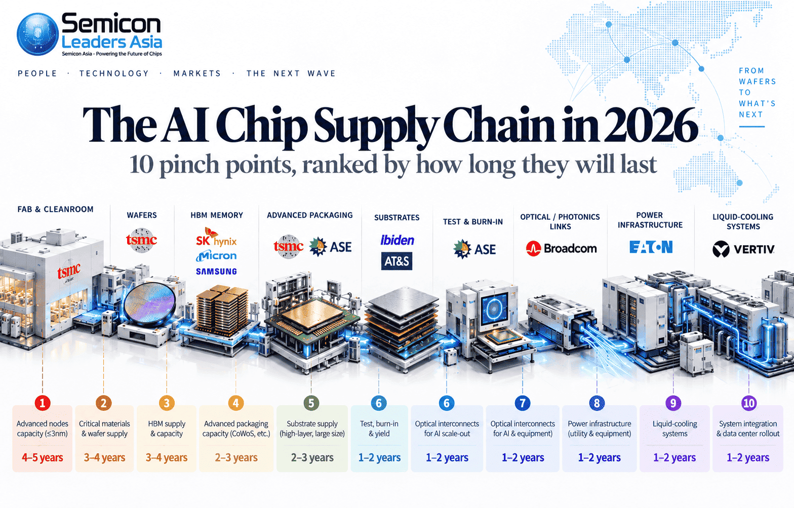
At Semicon Leaders Asia, we have therefore ranked ten AI supply-chain pinch points by duration, not simply by how painful they are today. The list counts down from the constraint most likely to ease first to the one with no clear end in sight.
How we ranked them
Severity today measures how strongly a constraint can limit AI-system shipments in late 2026, on a scale of one to ten. Expected meaningful relief is our estimate of when added capacity, new architectures or wider supplier qualification should materially reduce the bottleneck. It does not mean the constraint disappears, and it does not mean prices fall. Who benefits identifies the companies or supplier groups with the strongest position while capacity remains scarce.
The ranking deliberately separates severity from duration. A 10/10 shortage that eases in eighteen months is a different business problem from an 8/10 shortage that lasts five years, and the second is often the one that reshapes industry structure.
The AI supply-chain constraint map
|
Rank
|
Pinch point
|
Severity today
|
Expected meaningful relief
|
Who benefits
|
|
10
|
Liquid cooling
|
6/10
|
H2 2027
|
Vertiv, Supermicro, thermal infrastructure suppliers
|
|
9
|
Leading-edge wafers
|
8/10
|
H2 2027, broader relief in 2028
|
TSMC and leading-edge equipment suppliers
|
|
8
|
CoWoS-class packaging
|
9/10
|
H2 2027
|
TSMC, ASE, advanced-packaging equipment suppliers
|
|
7
|
Test capacity
|
8/10
|
2028
|
ASE and specialist test suppliers
|
|
6
|
HBM
|
10/10
|
2028
|
SK hynix, Micron, Samsung
|
|
5
|
Advanced substrates
|
8/10
|
2028
|
Ibiden, AT&S and qualified substrate suppliers
|
|
4
|
Photonics
|
6/10
|
2028 to 2029
|
Broadcom and optical component suppliers
|
|
3
|
Power delivery
|
8/10
|
2029 and beyond
|
Eaton, ASE, Vertiv and power-component suppliers
|
|
2
|
Cleanroom construction
|
9/10
|
2029 to 2030
|
Semiconductor equipment and construction ecosystems
|
|
1
|
Skilled labour
|
8/10
|
No clear relief before 2030
|
Established manufacturing clusters and employers with trained teams
|
Source note: The severity scores, ranking and relief dates are Semicon Leaders Asia estimates based on company capacity plans, earnings commentary and SEMI industry data. They are not company guidance.
10. Liquid cooling: capacity is being added fast enough to matter
Severity today: 6/10 | Expected relief: H2 2027
What happened
Rack power density has moved beyond what conventional air cooling can handle comfortably. As a result, coolant distribution units, chillers, cold plates and facility plumbing have become part of the AI hardware supply chain rather than a line item in a building contract.
The industrial response has been unusually fast. Vertiv expects expansion at its Tognana operation in Italy to double regional chiller production capacity by the end of 2026, while a roughly US$50 million Ohio expansion for liquid-cooling and chilled-water systems is due to become operational in Q2 2027. Its new Johor operation is also adding thermal and power manufacturing capacity for Asia, close to one of the region's fastest-growing data-centre corridors.
Why it matters
Cooling remains a real deployment constraint, but unlike a semiconductor fab, most of the hardware is fabricated metal, pumps, heat exchangers and controls. That manufacturing can be scaled in quarters, not years. The harder part is integration at the data centre: retrofitting halls designed for air, securing water and heat-rejection permits, and commissioning systems that cannot be allowed to leak beside equipment worth millions of dollars per rack.
What to watch in 2027
Watch whether equipment availability stops being the problem and site readiness becomes the bigger delay. Vertiv and Supermicro should benefit as buyers increasingly purchase cooling as part of an integrated rack or data-centre architecture rather than as an add-on. Suppliers that can deliver pre-integrated, factory-tested liquid-cooled racks will capture more value than those selling components.
9. Leading-edge wafers: very tight, but capacity has a visible arrival date
Severity today: 8/10 | Expected relief: H2 2027, broader relief in 2028
What happened
TSMC says AI demand remains extremely strong and that the supply gap is still large. Yet the capacity response is unusually visible. N2 annual capacity is expected to more than double in 2027. A new 3nm fab in Tainan is due to begin volume production in the first half of 2027, while TSMC's second Arizona fab is scheduled for volume production in Q3 2027.
Why it matters
Leading-edge wafers are scarce, but this is fundamentally a capital-and-tool problem, and the capital is already committed. The tools are ordered, the shells are going up and the process recipes exist. SEMI's forecast of continued growth in 300mm equipment spending through the end of the decade supports the same conclusion: the industry knows how to add this capacity, and it is doing so.
There is a concentration risk that buyers should not ignore. Nearly all of the world's most advanced AI logic still flows through a single foundry, and most of that through Taiwan. Additional overseas fabs widen the geographic base, but they do not yet change who controls the leading edge.
What to watch in 2027
The important number is not fab announcements. It is usable N2 and N3 wafer output. If yield ramps and tool installation follow schedule, wafer scarcity should become less dominant relative to packaging, memory and infrastructure. A slip in N2 yields, or a sudden jump in custom accelerator tape-outs, would push relief into 2028.
8. CoWoS-class packaging: capacity is rising, but package size keeps moving the target
Severity today: 9/10 | Expected relief: H2 2027
What happened
TSMC says CoWoS remains its customers' leading advanced-packaging choice. It is already producing packages of around five reticle sizes and is developing nine-reticle and 14-reticle approaches.
ASE is simultaneously widening the alternative capacity pool. Its automated 310mm by 310mm panel-level packaging line, compatible with its FOCoS and FOCoS-Bridge technologies, is expected to enter production in 2027.
Why it matters
Capacity additions do not automatically eliminate the bottleneck, because every accelerator generation consumes more packaging area and more integration complexity. A package five times the reticle limit uses far more interposer area, carries more HBM stacks and has more opportunities for yield loss than one at twice the limit. The unit of demand is changing faster than the number of packages suggests, which is why CoWoS capacity can double and still feel tight.
Panel-level processing matters because a large square panel uses its area more efficiently than a round wafer when the packages themselves are very large. It is one of the few levers that changes the economics, rather than simply adding more of the same lines.
What to watch in 2027
Watch qualified capacity outside TSMC and the transition towards panel processing. If ASE and other OSATs take a meaningful share of high-end AI packages, the constraint should loosen. If package footprints keep expanding faster than throughput, advanced packaging will not disappear as a bottleneck. It will simply move from one process step to another.
7. Test capacity: the less visible back-end constraint
Severity today: 8/10 | Expected relief: 2028
What happened
On its Q2 earnings call, ASE said wafer-sort and final-test capacity were running near full, with capacity outside newly installed equipment generally close to full utilisation. Near-term growth was being gated by capital-equipment installation and facility build-out. The company added roughly US$2 billion to planned facilities and equipment spending as demand strengthened.
ASE is also building a NT$17.8 billion facility in Kaohsiung that incorporates high-end packaging and testing, but completion is scheduled for Q2 2028.
Why it matters
Test rarely makes headlines, yet it is where the economics of advanced packaging are protected. More chiplets and more HBM stacks mean more interfaces that have to work together, and a single faulty die discovered after assembly can scrap an entire package worth thousands of dollars. Test demand therefore grows with package complexity, not simply with unit volume. Test times are lengthening, power levels during test are rising, and handlers and thermal systems must cope with devices that draw far more current than earlier generations.
What to watch in 2027
Test time per package and equipment utilisation matter more than headline OSAT capacity. The beneficiaries are operators with both advanced-packaging and high-power, high-frequency test capability under one roof, along with specialist test-equipment suppliers. Because the Kaohsiung expansion lands in 2028, we expect test to remain tight for longer than packaging itself.
6. HBM: the worst shortage today is not necessarily the longest one
Severity today: 10/10 | Expected relief: 2028
What happened
SK hynix began mass shipments of HBM4 in Q2 2026 and says customer demand continues to exceed its supply capability. It is accelerating its M15X fab and plans to begin opening the first Yongin cleanroom in February 2027.
Micron spent US$27.37 billion on net capital expenditure in fiscal 2026 and has HBM4 in high-volume shipment, with HBM4E volume production planned for calendar 2027. Samsung, the third supplier, is fighting to expand its qualified share of the most demanding AI platforms.
SEMI forecasts memory fab equipment investment of US$52 billion in 2026 and US$57 billion in 2027.
Why it matters
HBM is severe because capacity cannot be added independently. Every HBM stack needs DRAM wafers, cleanroom space, through-silicon-via processing and advanced stacking, and each of those has its own lead time. Micron has said in the past that HBM consumes roughly three times the wafer supply of standard DRAM for the same number of bits, so every shift towards HBM also tightens the conventional memory market.
At the same time, memory content per accelerator keeps rising. Each new platform adds more stacks, more layers per stack and higher speeds. Suppliers are expanding the pie while customers are asking for a bigger slice of it on every chip.
What to watch in 2027
The key question is whether new cleanroom and packaging capacity grows faster than HBM content per accelerator. We expect the shortage to improve, but not normalise, during 2027. HBM ranks only sixth by duration because the relief mechanism is clear: the three memory makers know how to build this capacity, they have the cash flow to fund it and the cleanrooms are already under construction. Pricing power will stay with the suppliers until those cleanrooms are full of qualified tools.
5. Advanced substrates: the bottleneck underneath the package
Severity today: 8/10 | Expected relief: 2028
What happened
Ibiden says demand for AI-server IC package substrates exceeds its capacity and has approved approximately ¥500 billion of electronics investment from FY2026 through FY2028. New capacity at its Gama site is scheduled to come online progressively from FY2027.
AT&S has separately agreed with AMD and another customer on capacity expansion in Kulim, Malaysia, backed by long-term customer commitments. Planned investment is €1.5 billion to €2 billion, with FY2026/27 capital expenditure lifted to €1 billion to €1.2 billion.
Why it matters
AI substrates are not interchangeable with the smaller products built during previous capacity cycles. Larger body sizes, more build-up layers, finer line spacing, tighter warpage tolerances and heavier power-delivery requirements all consume more process capacity per package. A substrate line that comfortably served PC processors cannot simply be redirected to AI accelerators.
The customer behaviour is also telling. When a chip designer co-funds a substrate maker's factory in exchange for committed capacity, as at Kulim, it signals that buyers no longer expect to secure supply on the spot market.
What to watch in 2027
Watch whether announced capacity reaches qualified volume on schedule. Qualification of a new substrate line for a flagship accelerator can take many months after the line itself is running. We expect substrates to remain one of the strongest pricing points below the headline chip through 2028, with glass-core substrates emerging as the next technology transition to track.
4. Photonics: not yet the biggest shortage, but increasingly structural
Severity today: 6/10 | Expected relief: 2028 to 2029
What happened
Broadcom's AI semiconductor revenue reached US$16.7 billion in fiscal Q3 2026, up 221% year on year, showing how rapidly custom accelerators and networking are scaling together.
At the physical layer, Broadcom is already shipping production co-packaged optics systems and introduced a 400G-per-lane 3nm optical DSP in March. An industry consortium formed in 2026 to establish an open optical scale-up specification for AI infrastructure.
Why it matters
Photonics is a different kind of constraint from HBM. The problem is not simply manufacturing more of the same component. AI clusters are moving towards a new interconnect architecture because copper reach and power consumption become increasingly difficult to manage as bandwidth rises. Moving optics from pluggable modules at the front of the switch onto the package itself changes how chips are designed, assembled, tested and serviced.
That transition involves lasers, silicon photonics, fibre attach, new packaging steps and new reliability standards. Each has a limited pool of qualified suppliers, and several depend on compound semiconductor materials with their own supply chains.
What to watch in 2027
Watch 1.6T optical deployments, co-packaged optics qualification and multi-vendor interoperability. The constraint persists because every network generation raises the bandwidth requirement again, and because architectural transitions take longer to industrialise than capacity expansions. Its severity today is moderate, but its duration is what earns it fourth place.
3. Power delivery: the bottleneck is moving from the board towards the grid
Severity today: 8/10 | Expected relief: 2029 and beyond
What happened
In October, ASE introduced an expanded PowerSiP platform that moves voltage regulation closer to the processor. The company says its vertical approach can reduce parasitic routing losses by 50% or more.
At the facility level, Eaton is expanding manufacturing for power distribution systems, including a new Virginia site expected to begin production in 2027. It has also developed grid-to-chip infrastructure designed specifically for next-generation AI factories.
Why it matters
Power is a constraint at every layer at once. Inside the package, more compute density means more current has to reach the processor with minimal loss. On the board and in the rack, power shelves, busbars and conversion stages must handle loads that would have powered an entire row a few years ago. At the site, the data centre needs utility-scale electrical capacity, transformers and switchgear, several of which carry multi-year lead times.
Solving one layer does not solve the others. A more efficient voltage regulator does not help a campus waiting years for a grid connection.
What to watch in 2027
Power availability will increasingly decide where AI accelerators can actually be deployed, even when the chips themselves are available. TSMC is already checking power-supply progress as part of its assessment of customers' data-centre build-outs, a striking sign of how far upstream the issue has reached. For Asia, the markets that can offer reliable grid capacity, competitive tariffs and fast permitting will win a disproportionate share of AI infrastructure investment.
2. Cleanroom construction: money cannot compress every lead time
Severity today: 9/10 | Expected relief: 2029 to 2030
What happened
SEMI expects 20 new 300mm fabs or lines to begin construction globally in 2026, and another 18 in 2027, with equipment spending continuing to rise through 2029.
SK hynix is accelerating its first Yongin cleanroom to February 2027, while Micron's new Singapore wafer fab will provide 700,000 square feet of cleanroom space, with wafer output not scheduled until the second half of 2028.
Why it matters
A cleanroom is the physical denominator beneath HBM, leading-edge logic and several other constraints on this list. Equipment can only be installed once qualified space, ultrapure water, specialty gas systems, vibration control and electrical infrastructure are ready. Those depend on specialised contractors, long-lead mechanical and electrical components, and permits.
With dozens of fabs being built simultaneously across Taiwan, Korea, Japan, Singapore, Malaysia, India, the United States and Europe, the specialist construction ecosystem is itself a scarce resource.
What to watch in 2027
Construction schedules matter as much as semiconductor equipment orders. A single delayed cleanroom can postpone hundreds of downstream tool installations at once, and the impact cascades into memory, logic and packaging output a year later. Track topping-out dates and first-tool move-in dates rather than groundbreaking ceremonies.
1. Skilled labour: the constraint capital spending cannot quickly solve
Severity today: 8/10 | Expected relief: no clear relief before 2030
What happened
SEMI estimates the semiconductor industry will need roughly one million additional skilled workers globally by 2030. Its workforce analysis points to shortages across engineers, technicians and experienced manufacturing leadership, with large gaps expected in both Europe and Asia-Pacific.
Why it matters
A new fab shell can be financed in one budget cycle. Yield engineers, packaging specialists, equipment technicians and experienced operations managers cannot. It takes years to train a competent process engineer, and longer still to develop someone who can ramp a new node or bring a struggling line back to target yield.
The problem is sharper because capacity is spreading beyond established Asian clusters. The industry is simultaneously building leading-edge fabs, HBM lines, advanced-packaging operations, substrate plants and AI data centres in more locations than ever before. Each new site needs a core of experienced people, and most of those people currently work in a small number of places.
What to watch in 2027
Watch hiring, retention and how aggressively companies move experienced teams between sites. Established clusters in Taiwan, South Korea and Japan retain an advantage that does not appear on a capex spreadsheet: experienced people already working inside dense supplier ecosystems. Emerging hubs, from Malaysia and Singapore to India and Vietnam, will need sustained investment in university programmes, technician training and immigration policy to close that gap. Labour ranks first not because it is the most acute shortage today, but because nobody can credibly name the date it ends.
What this means for Asia
Asia sits at the centre of almost every constraint on this list. Taiwan dominates leading-edge logic and CoWoS-class packaging. South Korea leads HBM. Japan is critical in substrates, materials and equipment. Southeast Asia is fast becoming the expansion ground for substrates, back-end assembly and data-centre infrastructure, with Malaysia, Singapore and others drawing new investment.
That concentration is both an advantage and a risk. The region captures much of the value created by scarcity, but it also carries the burden of building the cleanrooms, grid capacity and talent pipelines that the structural constraints demand. Governments that focus incentives on the long-duration bottlenecks, particularly power, construction capability and skills, are likely to see more durable returns than those that chase the shortage making headlines this quarter.
Semicon Leaders Asia view
The important distinction in 2026 is between cyclical scarcity and structural scarcity.
Liquid-cooling hardware can be manufactured faster. Leading-edge wafer capacity has billions of dollars of committed expansion behind it. CoWoS-class packaging should broaden as TSMC adds capacity and OSAT alternatives mature. Those constraints can still hurt 2027 shipments, but they have visible relief mechanisms.
The harder problems sit underneath them. Advanced substrates require new manufacturing capability for increasingly large and complex packages. Photonics requires an architectural transition, not simply another factory. Power delivery reaches from the package all the way to the grid. Cleanrooms take years to build. Skilled labour takes longer still.
HBM sits between the two groups. It is probably the most severe constraint today, but not the longest-lasting one. Massive spending by SK hynix, Micron, Samsung and their equipment suppliers should eventually create more supply. The complication is that AI memory content keeps increasing while that capacity is being built.
For buyers, the implication is straightforward: do not treat every shortage with the same procurement strategy. A constraint expected to ease within twelve to eighteen months can justify capacity reservations and temporary premiums. A structural constraint requires something different: second sources, long-term agreements, co-investment, design changes or geographic diversification.
For investors, the same distinction matters. The most durable beneficiaries of the AI build-out may not be the suppliers attached to the loudest shortage of 2026. They may be the companies controlling the capacity that takes longest to reproduce.
The next phase of the AI semiconductor cycle will therefore be decided less by which bottleneck is tightest today, and more by which one still has no easy answer when the new fabs open.
Sources
- TSMC, Q3 2026 earnings call transcript | https://investor.tsmc.com/english/encrypt/files/encrypt_file/reports/2026-10/eba4fac72873bf546b669bd2b5d973df5c93215d/TSMC%203Q26%20Transcript.pdf
- SEMI, Global 300mm fab equipment spending to reach US$227 billion in 2029 | https://www.semi.org/en/semi-press-release/global-300mm-fab-equipment-spending-to-reach-227-billion-in-2029-as-buildout-accelerates-semi-projects
- SEMI, 300mm memory equipment investment to surpass US$50 billion in 2026 | https://www.semi.org/en/semi-press-release/semi-projects-300mm-memory-equipment-investment-to-surpass-50-billion-dollars-in-2026
- SEMI, The semiconductor talent crisis | https://www.semi.org/en/blogs/the-semiconductor-talent-crisis-why-growing-demand-cant-find-leaders
- ASE Technology, Form 6-K filing (Q2 2026) | https://www.sec.gov/Archives/edgar/data/1122411/000095010326011351/dp250868_6k.htm
- ASE Technology, Q2 2026 earnings call transcript (StockAnalysis) | https://stockanalysis.com/quote/tpe/3711/transcripts/656634-q2-2026/
- ASE, 310mm x 310mm panel-level packaging line | https://www.aseglobal.com/press-room/310x310/
- ASE, New high-tech facility in Kaohsiung | https://ase.aseglobal.com/press-room/ase-breaks-ground-on-new-high-tech-facility-in-kaohsiung/
- ASE, Expanded PowerSiP platform | https://ase.aseglobal.com/press-room/ase-expands-powersip-platform-for-next-generation-ai-power-delivery/
- SK hynix, Q2 2026 business results | https://news.skhynix.com/en/q2-2026-business-results/
- SK hynix, New facility investment for Yongin semiconductor cluster | https://news.skhynix.com/en/new-facility-investment-for-yongin-semiconductor-cluster/
- Micron, Quarterly results | https://investors.micron.com/financials/quarterly-results/default.aspx
- Ibiden, FY2025 Q3 Q&A | https://www.ibiden.com/ir/items/en_QA_FY2025Q3.pdf
- AT&S, AI substrate capacity expansion in Kulim | https://ats.net/en/ir-news/ats-expands-ai-substrate-capacity-in-kulim-and-increases-outlook-for-2026-27/
- Broadcom, Q3 FY2026 financial results | https://investors.broadcom.com/news-releases/news-release-details/broadcom-inc-announces-third-quarter-fiscal-year-2026-financial
- Broadcom, Co-packaged optics | https://www.broadcom.com/info/optics/cpo
- Eaton, New Virginia facility | https://www.eaton.com/us/en-us/company/news-insights/news-releases/2025/eaton-invests-fifty-million-dollar-in-new-virginia-facility.html
- Vertiv, Global manufacturing expansion for AI-ready cooling | https://www.vertiv.com/en-in/about/news-and-events/news-releases/2026/vertiv-expands-global-manufacturing-capacity-for-ai-ready-data-center-cooling-solutions/