Diamond Foundry Develops 200mm Single-Crystal Diamond Wafer for Advanced Semiconductor Applications
20 November 2026 |
Interaction
The breakthrough could open new possibilities for AI chip cooling, high-power electronics and future diamond-based semiconductors, with the company targeting 300mm wafer production by 2030.
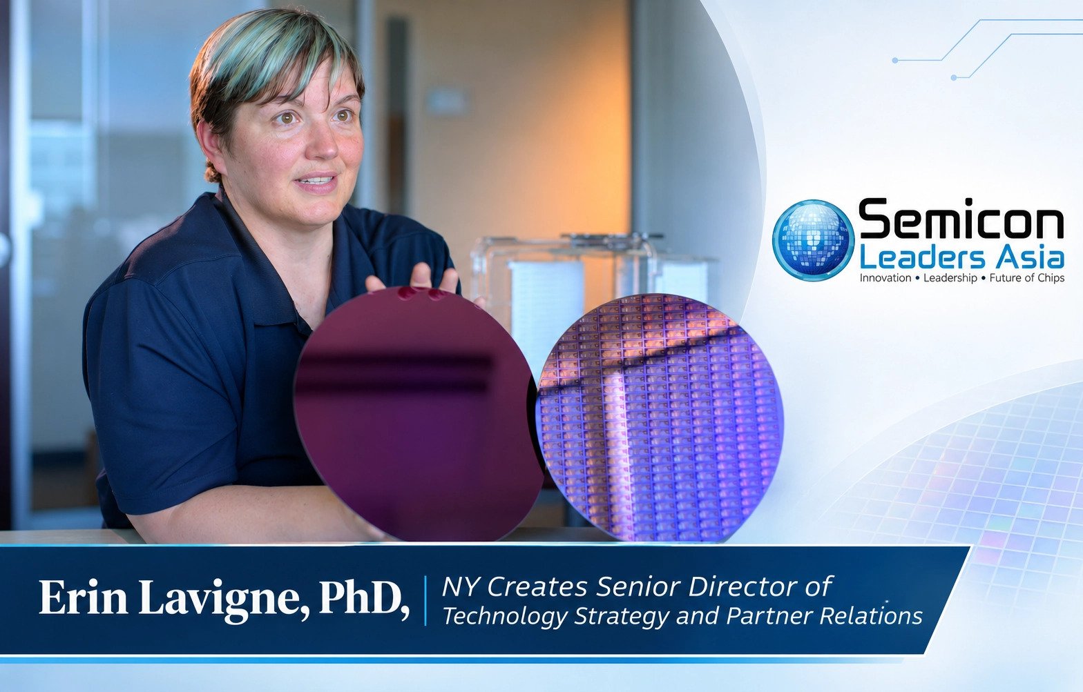
As AI processors become more powerful, managing heat is emerging as a major challenge for semiconductor manufacturers. Diamond Foundry has developed a 200mm single-crystal diamond wafer, marking a step towards using diamond in mainstream chip manufacturing. The company sees near-term opportunities in thermal management, with longer-term ambitions for diamond transistors and larger wafer production. Semicon Leaders Asia speaks with Jeff Yurek, VP Marketing, Diamond Foundry about the technology behind its 200mm breakthrough, its potential for AI chip cooling, manufacturing scalability and the roadmap towards commercial production.
Q. Diamond Foundry has achieved a major milestone by developing the first 200mm single-crystal diamond. What makes this achievement important for the company, and how could it create new opportunities in the semiconductor industry?
Once every few decades, a new single-crystal wafer comes along. Silicon got its first in 1959, and most of modern technology was built on it. Now we have diamond, with a physics far superior to that of any other semiconductor.
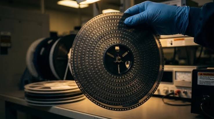
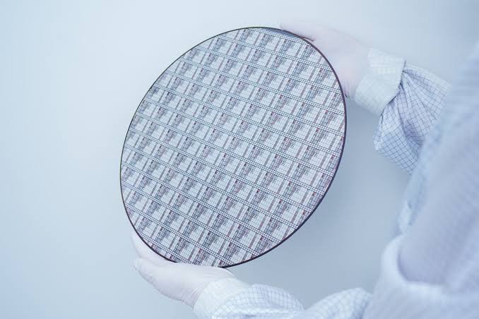
D200 is one continuous crystal of diamond, 200mm across. Not tiles stitched together, and not polycrystalline diamond. That puts single-crystal diamond in the dimensions the semiconductor industry is built around.
For the semiconductor industry it matters in two ways: diamond behind every chip for thermal reasons, as a substrate that pulls heat out of high-power processors, and diamond as the chip itself, with diamond transistors.
Q. Diamond has long been considered a promising material for advanced electronics, but its limited size has restricted wider adoption. What were the biggest challenges in producing a 200mm single-crystal diamond, and how did Diamond Foundry overcome them?
We had to create the mother of all single-crystal diamond wafers, on a growth substrate that is not diamond: diamond heteroepitaxy.
There is only one group of scientists in the world that understands the science and technology for making diamond heteroepitaxy work across scalable substrate area — and we acquired that group in Augsburg, Germany in 2021.
Combined with hundreds of engineers at DF, this has now yielded the first wafer-sized SCD.
The tech here is about controlling how ten atoms of carbon meet a non-diamond substrate and form a single crystal — using custom high-vacuum equipment of a kind never built before.
Q. As AI processors become more powerful, managing heat is becoming a major challenge for chipmakers. How could diamond’s thermal properties help improve chip performance, energy efficiency and reliability?
Hotspots are evil. A chip can be cool on average and still too hot in the tensor cores and the circuitry around them. The hottest spot sets how fast the chip can run, and heat accelerates a plethora of failure mechanisms. A standard reliability rule of thumb: every 10°C of sustained junction temperature can roughly halve lifetime for a typical wear-out mechanism.
Diamond flattens the peak. Our single-crystal diamond substrates have 20 times the thermal conductivity of silicon. Bonded within microns of the transistors, they spread heat sideways before it piles up, and give the cooling system more area to work with. In chips tested in fabs, we’ve measured temperature reductions of up to 52°C. 52 degrees. That is a fundamentally different thermal envelope.
Chip designers can spend that enhanced thermal envelope on performance, on lifetime, or on a mix of both. Cooler silicon also leaks less current, so more of every watt goes into computation.
For datacenters, the number that matters is lifetime tokens per dollar of capital invested. A $30,000 accelerator that runs reliably for six years instead of two or three changes the economics of the whole facility. That’s what we mean by making AI chips bankable.
Q. The company aims to make single-crystal diamond available at semiconductor-relevant wafer sizes. What steps are needed to move from this successful demonstration to commercial-scale manufacturing, and what challenges remain?
It will happen faster than most expect — because we have already deployed D200mm SCD ingot growth reactors at scale around the world.
Q. Diamond Foundry sees opportunities for its technology in AI computing, high-power electronics, optics and quantum systems. Which of these applications offers the strongest near-term market potential, and what kind of interest are you seeing from semiconductor companies?
Thermal for AI chips is a big focus near term.
Hotspots limit how fast accelerators can run and how long they last. Our chip-size substrates exist today at the full ASML reticle size.
Chip designers have known for decades that diamond is the ultimate material. They just never thought they could get hold of it. Now it exists.
Q. Following the successful development of the 200mm crystal, Diamond Foundry has indicated that 300mm single-crystal diamond could be achievable. What are the company’s next development priorities, and how do you see diamond becoming part of mainstream semiconductor manufacturing in the future?
D200 makes D300 predictable now. We went from 100mm straight to 200mm, skipping 150mm.
We have already designed and built six of the seven reactor types required to create the mother of all D300mm single-crystal diamond wafers.
The process and reactor technology that got us to D200 compounds from one generation to the next.
We have a “Five Threes” wafer roadmap: 3 million wafers, 300mm in diameter, 3,000 W/m·K thermal conductivity at $3 per carat, or cost parity with silicon carbide — by 2030.
Cost is where diamond surprises people. We crystallize greenhouse gas into diamond. The byproducts are oxygen and water, with no toxic gases or silanes required to be managed. Consumables cost is effectively zero. Simplicity is why diamond will ultimately be much cheaper than silicon carbide.
Mainstream means two things. First, diamond behind every chip: the AI chips of the future will be 99% diamond, counting the atoms. Then, further out, diamond as the chip itself.