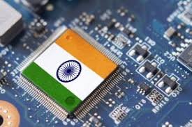
India’s Semiconductor Revolution Finds Its Backbone in Materials Science
As India races to join the global semiconductor elite, the quiet catalysts—bonding wires, solder pastes, fluxes, and adhesives—are emerging as the real enablers of its chipmaking future, drawing global giants like Tanaka and Indium Corporation to build the foundations of a resilient materials ecosystem.
As India’s semiconductor aspirations gather pace, the spotlight is gradually shifting from fabrication plants to the unsung enablers of the chipmaking process — the materials that make every connection possible.
From bonding wires and solder pastes to fluxes and adhesives, global materials manufacturers are homing in on India, viewing it as a future hub not just for chip assembly, but also for the critical components that determine whether a semiconductor can withstand heat, conduct current, and support advanced 2.5D and 3D packaging.
The Missing Link in India’s Semiconductor Chain
While India boasts a respectable base of local suppliers for electronics-grade soldering consumables, the domestic production of ultra-fine, high-purity chip-grade materials — essential for next-generation semiconductor packaging — remains limited. Most high-precision materials are still imported, and local R&D is at an early stage.
“Bonding wires are indispensable in OSATs [Outsourced Semiconductor Assembly and Test facilities] to connect the integrated circuit (IC) with the substrate. They form the direct link inside the IC,” explained Agus and Fushimi, technical representatives at Tanaka Precious Metal Technologies Co., Ltd. “Silver adhesive, used for die attachment between silicon chips and lead frames, provides both thermal conductivity and electrical reliability. It is also used in power semiconductors for mounting silicon chips directly onto copper substrates.”
They added, “Sputtering targets — made from precious metals such as gold, platinum, and palladium — are critical in forming thin films in front-end processes. Each metal or alloy contributes unique properties essential to chip performance.”
India’s Appeal: Early Moves and Global Entrants
Under the India Semiconductor Mission (ISM), the government has managed to attract not only potential fab investors but also suppliers from across the semiconductor value chain. Among them, Tanaka and Indium Corporation stand out — both betting on India’s long-term rise in packaging, assembly, and materials technology.
Tanaka: From Precious Metals to Semiconductor Ecosystems
With over 30% of the global bonding wire market, Tanaka is now actively expanding in India. Its local subsidiary, Tanaka Kikinzoku (India) Pvt. Ltd., established in Mumbai in 2020, initially served the automotive industry. Now, semiconductor packaging has become its next frontier.
“We see a clear opportunity to bring our complete materials ecosystem to India,” said Yutaka Ito, Managing Director of Tanaka India. “Precious metals are finite yet indispensable, which is why recycling them from e-waste into new materials forms the foundation of our business. India’s growth and scale make it ideal for this closed-loop model.”
Tanaka predicts that by 2026–2030, most OSATs operating in India will have functional facilities — with capacity likely to double by the end of the decade.
Indium Corporation: Building From the Ground Up
Meanwhile, Indium Corporation, which operates a manufacturing facility in Chennai producing high-end solder pastes, is equally bullish.
“We are proud of our Chennai factory and optimistic about the future of both PCBA [Printed Circuit Board Assembly] and semiconductor packaging in India,” said Ross Berntson, CEO of Indium Corporation. “Our initial investment was driven by logistics — solder paste is perishable. But our long-term vision is rooted in India’s potential as both a demand centre and an innovation hub.”
Indium specialises in developing custom alloys and fluxes collaboratively with its customers. “Our uniqueness lies in the way we co-develop solutions,” Berntson noted. “A client presents a technical problem, we engineer a solution, and once proven, it often becomes a global standard.”
Among its recent breakthroughs is Durafuse LT solder, originally designed for low-temperature assembly but now gaining traction in AI packaging and telecom, as well as e-mobility and thermal management.
Early Challenges, Emerging Opportunities
India’s journey toward self-sufficiency in advanced semiconductor materials is not without challenges. Infrastructure gaps — especially concerning recycling refineries, stable electricity, and ultra-pure water — remain obstacles.
“Stable electricity and pure water are essential to sustain refining capabilities,” Ito observed, adding that Tanaka aims to localise its closed-loop metal recycling process once those foundations strengthen.
Indium, meanwhile, is already planning to go beyond manufacturing into local R&D. “We envision establishing a research team in India,” Berntson said. “What stands out to me is the willingness to collaborate. Customers here are eager to iterate and solve problems with us — a sign of a maturing innovation culture.”
Laying the Groundwork for India’s Semiconductor Future
Both Tanaka and Indium are positioning themselves ahead of India’s upcoming wave of semiconductor packaging and OSAT facilities, many of which are expected to enter pilot production by 2026.
Tanaka’s portfolio already includes 29 variants of bonding wires, tailored for different loop heights, strengths, and materials — including silicon carbide (SiC) applications — while its silver pastes are optimised for copper lead frames. Indium, on its part, continues to expand into thermal management and e-mobility segments, building partnerships with Indian universities to deepen local expertise.
As India’s first large-scale semiconductor facilities move closer to reality, global materials specialists are quietly securing their footholds. For Tanaka and Indium, India is more than a fast-growing market — it is a testbed for long-term collaboration in materials science and an opportunity to co-create the backbone of the country’s chipmaking revolution.