Semiconductor Packaging Services Market to Reach US$118.59 Billion by 2035
AI, HBM, chiplets and advanced packaging technologies are driving strong growth as demand for high-performance and energy-efficient semiconductor solutions accelerates.
The global semiconductor packaging services market is expected to expand significantly over the coming decade as rising demand for artificial intelligence (AI), high-performance computing (HPC), high-bandwidth memory (HBM) and chiplet-based architectures increases the need for sophisticated packaging and testing capabilities. According to DataM Intelligence, the market was valued at US$44.50 billion in 2025 and is forecast to reach US$118.59 billion by 2035, representing a compound annual growth rate (CAGR) of 10.3% between 2026 and 2035.
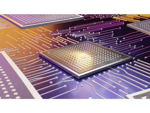
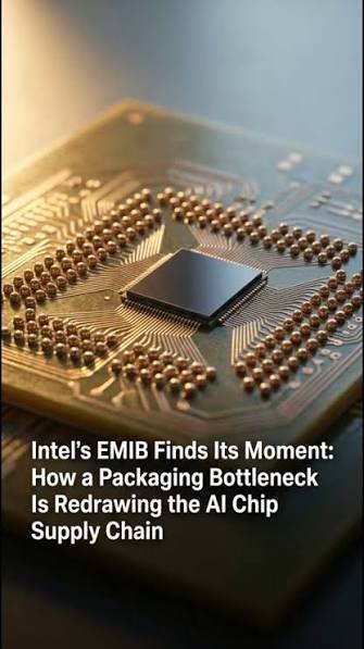
Semiconductor packaging is becoming an increasingly strategic part of chip development as manufacturers seek to deliver greater computing performance, improved energy efficiency and higher functionality within increasingly compact system designs. Packaging services cover key activities such as semiconductor assembly and testing, with providers supporting a wide range of package formats, materials and end-use applications.
The rapid expansion of AI infrastructure is emerging as one of the most important factors influencing the market. Modern AI processors require increasingly sophisticated methods to connect compute dies, memory and other components while maintaining high bandwidth and managing power and thermal requirements. This is driving greater interest in advanced packaging technologies, HBM integration, high-density interconnects and heterogeneous integration.
Chiplet architectures are also reshaping semiconductor packaging requirements. Instead of integrating all functions on a single large die, chiplet-based designs allow multiple specialised semiconductor components to be combined within one package. This approach can provide greater design flexibility and allow chipmakers to integrate different technologies and process nodes according to specific application requirements.
As chiplet adoption increases, packaging providers are being called upon to support increasingly complex multi-die architectures. Advanced interconnect technologies and heterogeneous integration are therefore becoming important areas of investment as semiconductor companies look to scale performance without relying solely on conventional monolithic chip designs.
Another technology receiving increased attention is panel-level packaging. Larger-format packaging approaches can potentially improve material utilisation and manufacturing efficiency while supporting increasingly complex package structures. According to the market report, initiatives from major industry participants are demonstrating the growing interest in panel-level approaches for chiplets, ASICs and HBM-oriented AI and HPC applications.
The competitive landscape is also evolving as semiconductor companies and outsourced semiconductor assembly and test (OSAT) providers increase cooperation. Recent developments highlighted by DataM Intelligence include expanded collaboration between NVIDIA and Amkor Technology on advanced packaging and testing for AI and accelerated computing, as well as initiatives by ASE Technology to develop automated panel-level packaging capabilities.
Strategic cooperation between packaging providers and semiconductor manufacturers is becoming increasingly important as customers seek access to specialised packaging capacity, testing expertise and advanced integration technologies. Such partnerships are also helping companies address the growing complexity of next-generation semiconductor architectures while improving manufacturing scalability.
The market is divided across several service and technology categories. Assembly and testing remain core service areas, while packaging formats include dual inline packages, quad flat no-lead packages, ball grid arrays, chip-scale packages and flip-chip solutions. More advanced package architectures are gaining importance where applications demand greater integration density, electrical performance and space efficiency.
Material selection is another important factor, with plastic, ceramic and metal materials used according to requirements such as thermal management, electrical performance, reliability and operating environment. At the application level, demand comes from consumer electronics, automotive, healthcare, telecommunications and networking, aerospace and defence, data centres and computing, industrial and IoT systems, and power and energy applications.
Consumer electronics currently represents the largest end-use segment, accounting for 28.2% of the market, according to DataM Intelligence. However, the increasing deployment of AI infrastructure and data-centre computing is creating new opportunities for packaging companies, particularly in technologies supporting high-performance processors, HBM and multi-die integration.
Asia-Pacific Maintains Leading Position
Asia-Pacific remains the dominant region in the semiconductor packaging services industry, benefiting from its established semiconductor manufacturing infrastructure, extensive OSAT ecosystem, skilled workforce and well-developed electronics supply chain. Taiwan, China, South Korea and Japan continue to play important roles across semiconductor packaging, testing, materials and equipment.
The region's strong position is also supported by its concentration of semiconductor manufacturing and electronics production. As demand for AI accelerators, advanced memory and sophisticated computing systems increases, the established packaging ecosystem across Asia-Pacific provides manufacturers with access to specialised capabilities and supporting suppliers.
North America, meanwhile, is strengthening its domestic semiconductor packaging infrastructure through new manufacturing investments, government-backed semiconductor initiatives and greater cooperation between chip designers, foundries and packaging providers. Growth in AI computing, cloud infrastructure, automotive electronics and defence systems is contributing to the expansion of regional demand.
Europe is also working to strengthen its semiconductor packaging capabilities through research programmes and industrial investments designed to improve regional supply-chain resilience. Automotive electronics, industrial automation, telecommunications and aerospace applications remain important markets for semiconductor packaging technologies.
AI and Advanced Integration to Shape Future Growth
The continued development of AI and HPC systems is expected to remain a major growth driver for semiconductor packaging services. Increasing processor complexity is placing greater demands on how dies, memory and other components are connected within a package, making advanced packaging a critical part of overall semiconductor system design.
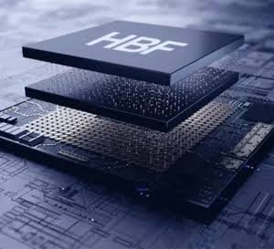
HBM is particularly important in this transition. AI accelerators require rapid access to large volumes of memory, increasing the need for packaging technologies capable of bringing high-bandwidth memory closer to processing units while addressing power, thermal and interconnect challenges.
At the same time, chiplets and heterogeneous integration are creating new opportunities for packaging service providers. As semiconductor designers increasingly divide complex systems into multiple dies, packaging becomes an important enabler of overall system performance rather than simply the final stage of chip manufacturing.
The market's projected growth therefore reflects a broader transformation in semiconductor development. Advanced packaging is increasingly being treated as a strategic technology that can influence computing performance, energy efficiency, manufacturing flexibility and system-level integration.
With AI infrastructure, data centres, automotive electronics, connected devices and advanced consumer products continuing to expand, demand for semiconductor packaging and testing services is expected to remain strong. The combination of HBM, chiplets, heterogeneous integration, high-density interconnects and emerging panel-level technologies is likely to play a central role in shaping the next phase of the packaging industry.