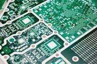
OKI Circuit Technology Develops 180-Layer PCB Technology for Next-Generation AI and HBM Testing
Breakthrough ultra-high multilayer boards will support advanced wafer test systems, with mass production targeted for October 2026 amid rising AI semiconductor demand

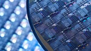
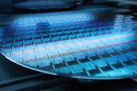
OKI Circuit Technology (OTC; President: Masaya Suzuki; Head office: Tsuruoka City, Yamagata), the OKI Group’s printed circuit board (PCB) business company, has successfully developed design and production technologies for 180-layer, 15 mm-thick PCBs intended for use in wafer testing equipment for high bandwidth memory (HBM) (Note 1) mounted on AI semiconductors. This represents an approximate 45% increase in layer count and approximately doubled board thickness compared to the previous 124-layer, 7.6 mm-thick configuration. OTC is pushing ahead with establishing mass production technology and setting up the required equipment at its Joetsu Plant, with the aim of starting mass production and shipment in October 2026. The plant, located in Joetsu City, Niigata Prefecture, has a proven track record and advanced development and production capabilities in the field of high multilayer, high-precision, large-format PCBs for semiconductor testing equipment.
Due to the enormous number of signals handled by the latest AI semiconductors, as well as the rising number of chips mounted on wafers accompanying process miniaturisation, PCBs for testing equipment must feature ever higher densities (reduced pitches) and layer counts. However, increasing the board thickness makes the characteristic impedance (Note 2) of vias (Note 3) more difficult to control; the power supply performance drops due to vias passing through power supply layers; and the drilling process for accurately boring fine, deep via holes involves technical limitations. Due to these constraints, the practical limits for single ultra-high-multilayer PCBs to address all these challenges had been 124 layers and 7.6 mm thickness, unable to meet future demand for high-speed, high-frequency, and high-density data transfer.
This time, OTC developed two technologies: Sintering Paste for Via Bonding, a conductive paste inter-substrate via bonding technology that allows multiple multilayer PCBs to be stacked and connected (by joining the vias on their surfaces); and a technology for manufacturing ultra-high-thickness PCBs measuring up to 15 mm thick. OTC combined these two technologies to establish design and production technologies for proprietary 180-layer, 15 mm-thick PCBs formed by stacking and connecting three 60-layer PCBs. By addressing via characteristic control, signal quality, and power supply performance issues for each multilayer PCB using well-established conventional technologies, individual multilayer PCBs can be stacked, enabling both ultra-high multilayering and superior performance and quality. This technology provides customers with the performance and quality needed to meet future demand for high-speed, high-frequency, and high-density data transfer.
OTC has developed these new technologies with an eye on fields expected to see significant growth—AI semiconductors, AI servers, aerospace and defense, and next-generation communications. OTC will continue to adapt to technological advancements and actively work on further development of PCBs and manufacturing technologies.
OTC will exhibit at PCB East 2026 (Booth 313), to be held at the DCU Convention Center in Worcester, Massachusetts, from April 28 to May 1, 2026, where it will showcase these technologies.