Move2THz is a European collaborative initiative focused on developing a sustainable Indium Phosphide-on-Silicon (InPoSi) technology platform and supporting ecosystem to enable next-generation high-frequency semiconductor solutions for future mass-market sub-terahertz applications.
The project aims to overcome the limitations of conventional Indium Phosphide technologies by establishing a mature and scalable value chain capable of delivering commercially viable and environmentally responsible components. These innovations are expected to support emerging use cases in advanced wireless communications and sensing technologies.
Aligned with the European Green Deal and the European Union’s ambition to achieve climate neutrality by 2050, Move2THz integrates sustainability with efforts to strengthen Europe’s industrial resilience and global competitiveness in advanced semiconductor manufacturing.
At the core of the initiative is the development of a high-performance InPoSi platform designed to operate at frequencies approaching the terahertz range while significantly reducing dependence on scarce raw materials. This approach lowers the environmental footprint of semiconductor production and contributes to the transition towards a more circular and sustainable semiconductor industry.
Sustainability is embedded across the entire product lifecycle, from material sourcing and manufacturing through to operation and end-of-life recovery. The project focuses on reducing energy consumption, minimising the use of rare materials, building environmentally responsible supply chains and applying lifecycle assessment methods to measure environmental impact.
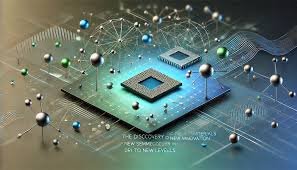
A key innovation within Move2THz is the substantial reduction in Indium Phosphide usage through advanced wafer bonding, smart-cut processes, and wafer reuse. By enabling donor wafers to be reused multiple times, the project significantly reduces raw material consumption while maintaining high performance. These advances demonstrate how cutting-edge semiconductor technology can deliver both industrial scalability and meaningful environmental benefits, reinforcing Europe’s position in the global semiconductor landscape.