Atomera, IQE Partner to Develop RF GaN-on-Silicon for Volume Manufacturing
The companies will combine Mears Silicon Technology and compound semiconductor epitaxy to develop lower-cost RF GaN wafers for foundries and chipmakers, with potential applications in power electronics.
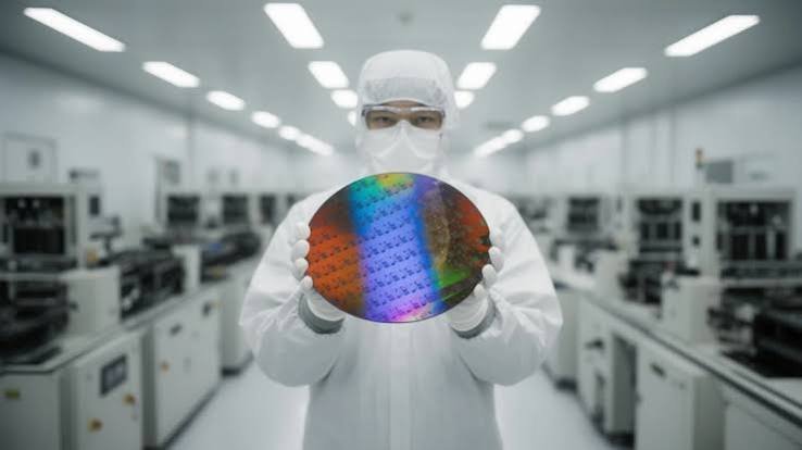
Atomera has signed a joint development agreement with IQE plc to develop gallium nitride-on-silicon (GaN-on-Si) wafers for radio-frequency (RF) semiconductor applications, targeting improved device performance and lower manufacturing costs in high-volume markets.
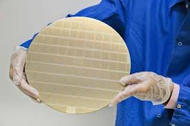
The collaboration will bring together Atomera's Mears Silicon Technology (MST) and IQE's compound semiconductor epitaxy capabilities to develop and evaluate GaN layers grown on silicon substrates.
Under the agreement, the companies will jointly optimise the material structure to improve RF signal linearity and reduce electrical losses. IQE is expected to manufacture MST-enabled GaN-on-silicon wafers for potential customers, including semiconductor foundries and integrated device manufacturers (IDMs).
The initial work will focus on producing and testing wafers that can meet the performance and cost requirements of mainstream RF applications.
Companies Target RF GaN Performance and Manufacturing Costs
Gallium nitride is increasingly used in RF and power semiconductor devices because of its ability to operate at high frequencies and support high power densities.
However, manufacturing high-performance GaN devices at competitive costs remains a challenge, particularly for applications requiring large production volumes.
High-performance RF GaN devices are commonly produced using silicon carbide substrates, which offer favourable thermal and electrical characteristics but are more expensive than silicon.
Silicon substrates provide a potentially lower-cost alternative and can support established semiconductor manufacturing processes. Their use in RF GaN devices, however, has been limited by electrical losses and material integration challenges that can affect high-frequency performance.
Atomera and IQE intend to address these limitations by combining specialised silicon material technology with advanced epitaxial growth processes.
The companies will evaluate how the resulting multilayer structures affect RF performance, particularly signal linearity and unwanted electrical losses.
Mears Silicon Technology Addresses RF Losses
At the centre of the development programme is Atomera's patented Mears Silicon Technology, an engineered epitaxial silicon layer designed to improve the electrical behaviour of semiconductor devices.
When incorporated into GaN-on-silicon structures, MST is intended to reduce unwanted electrical conduction at the interface between the GaN layers and the underlying silicon substrate.
Such parasitic conduction can increase RF losses, reduce power efficiency and limit device performance at higher operating frequencies.
In June 2026, Atomera reported test results showing that its MST approach reduced parasitic channel charge by more than tenfold in GaN-on-silicon structures.
The company said the results also demonstrated improvements in RF signal linearity, supporting its efforts to make silicon substrates suitable for a wider range of GaN applications.
The agreement with IQE represents a further development stage, moving from initial material demonstrations towards jointly optimised epitaxial wafers intended for customer evaluation.
IQE to Support Epitaxial Wafer Development
IQE will contribute its experience in compound semiconductor materials and epitaxial wafer manufacturing.
The companies expect development to proceed through several engineering cycles, during which their teams will adjust and test different material structures to identify suitable combinations for RF applications.
The programme will include wafer production, material characterisation and electrical performance testing.
Dr Rodney Pelzel, Chief Strategy and Technology Officer at IQE, said the collaboration would allow the company to assess MST-enabled silicon substrates as a potential foundation for RF GaN devices.
He indicated that the technology could offer a more economical substrate option while meeting the performance requirements of semiconductor customers.
The companies intend to make engineering samples available to foundries, IDMs and fabless semiconductor businesses for evaluation.
These samples will provide potential customers with an opportunity to assess the technology against their device design and manufacturing requirements.
Partnership Could Extend into Power Electronics
Although the initial development programme will concentrate on RF applications, the agreement also allows Atomera and IQE to examine other uses of GaN-on-silicon technology.
Power electronics is one potential area for further development, where GaN devices are being adopted for their high switching speeds and power efficiency.
Scott Bibaud, President and Chief Executive Officer of Atomera, said improving the economics of GaN manufacturing is important for extending the material beyond specialised applications.
He said IQE's manufacturing capabilities could help shorten the development process and support the transition of MST-enabled GaN-on-silicon wafers towards commercial supply.
For Atomera, the collaboration also provides an opportunity to extend the use of its licensed semiconductor materials technology into additional markets.
RF Semiconductor Market Looks Beyond Conventional Substrates
The collaboration comes as the semiconductor industry examines alternative material structures to meet the performance and cost requirements of future wireless communications systems.
RF GaN technology is relevant to applications including telecommunications infrastructure, high-frequency communications and other systems requiring efficient signal amplification.
Moving towards silicon-based substrates could offer cost and manufacturing advantages, provided the resulting devices can deliver the necessary electrical performance and reliability.
For foundries and semiconductor manufacturers, the key considerations will include wafer quality, process compatibility, manufacturing yields and the ability to maintain consistent RF performance across production batches.
The Atomera-IQE programme remains at the development stage, with no commercial production timetable or confirmed customer orders disclosed in the announcement.
The next milestone will be the production and evaluation of jointly developed wafers, followed by customer testing to determine whether the technology can meet the requirements of commercial RF semiconductor manufacturing.
If the partners can demonstrate suitable performance at competitive costs, MST-enabled GaN-on-silicon could provide another substrate option for manufacturers seeking to expand RF GaN production.