Great Lakes Semiconductor Launches Modular Fab and Advanced Packaging Project
The Great American ChipForge initiative brings together US and Japanese technology partners to develop AI-enabled automotive sensors through modular wafer fabrication, RISC-V processing and heterogeneous packaging.
Great Lakes Semiconductor (GLS) has announced the first project under its Great American ChipForge platform, bringing together semiconductor design, flexible wafer manufacturing and advanced packaging technologies to support the development of intelligent sensor systems for vehicles.
The project forms part of the company's Innovation Funnel initiative, which aims to move new semiconductor technologies from initial design through prototyping, testing and eventual commercial production.
The approach combines GLS design centres with its ChipForge modular wafer fabrication platform and FINPAT packaging and testing system. By connecting these activities, the company intends to reduce the time required to develop specialised semiconductor devices and prepare them for manufacturing.
GLS is working with several technology partners across Japan and the United States, covering equipment, sensors, memory, packaging and manufacturing planning.
GLS Brings Together Semiconductor and Packaging Partners
The project involves Neitas and Daikin of Japan, which will contribute modular semiconductor manufacturing equipment, alongside BlueDot Ventures, whose sensor technology portfolio has already been deployed in more than one million devices in commercial applications.
FMC will provide ferroelectric semiconductor memory technology, while Altascient will contribute predictive planning capabilities intended to support manufacturing and supply chain decisions.
Advanced Printed Electronic Solutions (APES) will lead work on additive electronics and packaging systems.
Within the FINPAT platform, APES plans to develop an additively manufactured package substrate capable of integrating semiconductor devices from GLS and FMC with several sensor technologies supplied by BlueDot Ventures.
The packaging approach is intended to bring computing, memory and sensing functions into a compact system while reducing power consumption and simplifying device integration.
ChipForge Uses Modular Wafer Manufacturing
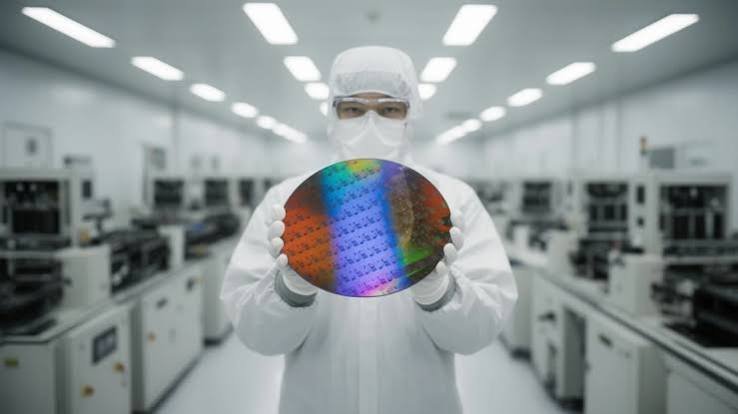
At the centre of GLS's strategy is ChipForge, a modular wafer fabrication platform designed to accommodate different semiconductor materials, manufacturing processes and device architectures.
Unlike conventional fabrication facilities built around a largely fixed production configuration, ChipForge is intended to allow individual manufacturing lines to be adapted to specific technologies and applications.
The company expects the platform to support products including logic devices, memory, processors, sensors and power semiconductors.
Potential markets extend beyond automotive electronics to defence, aerospace, healthcare, communications and industrial systems.
GLS said the modular design would allow manufacturers to introduce additional process equipment or new device technologies without undertaking a complete redesign of an existing fabrication facility.
The company also plans to connect specialised manufacturing lines within a coordinated network covering process development, fabrication, packaging, testing and supply chain operations.
Where technically feasible, processes validated through ChipForge could subsequently be transferred to larger manufacturing facilities operated by strategic foundry partners.
Dr Richard Thurston, Chairman and Chief Executive Officer of Great Lakes Semiconductor, said the project would demonstrate how closer integration between semiconductor design and manufacturing could shorten product development cycles.
He explained that GLS intends to align manufacturing processes and production requirements from the earliest design stages, allowing prototypes to be developed with commercial manufacturing considerations already in place.
Advanced Packaging Targets Low-Power Automotive Sensors
The first application will focus on integrating multiple sensor functions with low-power processing and memory technologies for vehicle systems.
BlueDot Ventures will contribute sensing devices based on technologies already deployed across commercial vehicle fleets.
Michael Sklansky, Chief Executive Officer of BlueDot Ventures, said practical sensor development depends heavily on controlling power consumption, device size, cost and reliability.
He said the partnership would allow the companies to combine sensing, communications and processing functions more closely within semiconductor packages.
A major part of the work will take place at the APES design centre in Fishkill, New York, where engineers are developing package substrates incorporating energy harvesting, supercapacitors and printed electronic components.
The proposed design will support a reusable power module that can accommodate different semiconductor and sensor combinations.
According to Dr Rich Neill, Chief Executive Officer of APES, the FINPAT manufacturing approach will bring together GLS power management devices, low-power RISC-V processors, FMC memory and BlueDot sensor technologies in a single packaged system.
The partners are also examining how ferroelectric memory could be placed close to an energy-efficient RISC-V processor running machine learning applications.
Such an arrangement could allow learned model data to remain stored while the processor enters a low-power state, reducing energy consumption in sensor applications that require intermittent processing.
GLS Plans to Shorten Semiconductor Development Cycles
Another objective of the project is to make it easier to modify semiconductor designs without restarting the entire manufacturing development process.
GLS and APES envisage a system in which engineers can adjust design parameters and produce alternative prototypes using established manufacturing processes, materials and design rules.
The approach could be particularly useful for smaller production volumes and specialised semiconductor applications where the cost of conventional manufacturing development can be difficult to justify.
The company intends to use its distributed design and manufacturing network to support projects from research laboratories, technology developers and industrial customers.
The broader GLS manufacturing strategy also includes plans for a PocketFab facility supporting prototypes and small production runs, alongside a full-scale 200 mm semiconductor manufacturing facility.
These facilities remain part of the company's development plans rather than completed manufacturing operations.
For the semiconductor industry, the project represents an attempt to link modular wafer fabrication with heterogeneous packaging, allowing specialised devices to move from design to production through a more closely integrated process.
The involvement of Japanese equipment suppliers and US semiconductor technology companies also highlights the role of international partnerships in developing regional semiconductor manufacturing capabilities.
The project's commercial impact will depend on whether GLS and its partners can demonstrate reliable production, repeatable processes and competitive manufacturing costs as the platform progresses towards commercial deployment.