EV Group Unveils EVG®40 D2W, First Dedicated Die-to-Wafer Overlay Metrology Platform for 300-mm Production
With 15× higher throughput and 100% die coverage, the EVG40 D2W enables precise, high-speed overlay measurement to improve yield and process control in advanced chiplet, HBM, and 3D SoC integration for AI and HPC applications.
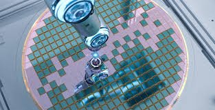
EV Group (EVG), a leading provider of innovative process solutions and expertise serving leading-edge and future semiconductor designs and chip integration schemes, today unveiled the EVG®40 D2W—the first dedicated die-to-wafer overlay metrology platform to deliver 100 percent die overlay measurement on 300-mm wafers at high precision and speeds needed for production environments. With up to 15X higher throughput than EVG's industry benchmark EVG®40 NT2 system designed for hybrid wafer bonding metrology, the new EVG40 D2W enables chipmakers to verify die placement accuracy and take rapid corrective action, improving process control and yield in high-volume manufacturing (HVM).
The EVG40 D2W can be used for any D2W bonding application, including chiplet integration, high-bandwidth memory (HBM) stacks, and 3D system on chip (SoC) integration processes, which enable high-performance devices for artificial intelligence (AI), high-performance computing (HPC), data centers and other applications. Multiple EVG40 D2W systems have already been installed at customer sites and are being used in HVM production services.
EVG executives will be available to discuss the EVG40 D2W system, as well as industry developments in chiplet integration, hybrid bonding and other important updates at SEMICON Taiwan, taking place this week in Taipei, Taiwan, September 8-12.
D2W Bonding Enables High-Performance Devices
D2W bonding integrates diverse dies or chiplets of different sizes, materials, and functions into a single device or package. This is essential for creating devices and systems that meet the increased performance demands of applications like AI and autonomous driving, with lower power consumption. As interconnect pitches in 3D packaging become tighter with each new product generation, die bond alignment and overlay processes must also scale accordingly, not only with greater accuracy but also higher measurement coverage, to identify overlay errors that can lead to misaligned copper pads or bond interfaces and result in yield loss.