Chuck Xu of Qnity on Enabling the Next Generation of AI Infrastructure Through Advanced Packaging Materials
29 June 2026 |
Interaction
Chuck Xu, President, Interconnect Solutions at Qnity, discusses how innovations in organic interposers, copper metallisation, dry film dielectric materials, and ecosystem collaboration are supporting the evolution of AI accelerators, high-performance computing, heterogeneous integration, and next-generation semiconductor packaging.
Q. AI-driven semiconductor architectures are placing unprecedented demands on advanced packaging. How do you see innovations in interposer materials influencing the next generation of AI accelerators, high-performance computing platforms, and heterogeneous integration strategies?
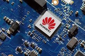
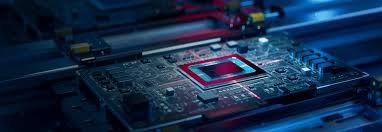
Advanced packaging has moved from a supporting role to a central driver of innovation in the semiconductor industry. As AI workloads, high-performance computing, and data-intensive applications require more processing power and efficiency, chipmakers are increasingly turning to advanced packaging technologies such as wafer-level packaging, panel-level packaging, interposer integration and 3D stacking to assemble chiplets, High Bandwidth Memory (HBM) and advanced node logic with new process materials, thermal solutions, and advanced interconnects.
Silicon interposers used in 2.5D packages such as CoWoS-S have been a mainstream solution for AI and HPC chips. However, the relatively high cost of silicon interposers, along with limitations in interposer size, has become a barrier to meeting next-generation requirements.
Organic interposers, incorporating copper redistribution layers (RDLs) and silicon bridges, are emerging as an effective alternative to address these challenges.
Advanced packages such as CoWoS-L, EMIB, and even panel-level packaging like CoPoS are adopting this concept. In this context, Qnity’s material innovations and technologies, including multi-role copper metallization and dry film photo-imageable dielectric materials, provide a strong fit to address market needs.
On the metallization front, by combining precise metallization processes with optimised materials and integration techniques, the solution supports finer line widths, tighter spacing, and improved signal integrity. To enable fine features, materials like Riston® dry film photoresists play a critical role in enabling next-generation advanced packaging on panel and IC substrate fabrication. Designed for high-resolution patterning and exceptional process reliability, these materials support the increasingly complex geometries required for high-density interconnects and miniaturised device architectures.
In addition, Qnity provides a comprehensive portfolio of solutions that support the full advanced packaging ecosystem, from wafer processing and interposer integration to IC substrates and final assembly.
Q. Qnity has introduced new copper metallization and dielectric solutions for organic interposer and glass substrate applications. How important is collaboration with foundries, OSATs, substrate manufacturers, and equipment suppliers in accelerating the commercial adoption of these advanced packaging technologies?
Qnity works closely with leading foundries, OSATs, and substrate manufacturers to develop next-generation solutions that meet evolving customer requirements for higher performance and broader process windows.
Through early engagement and close collaboration, Qnity’s R&D teams work directly with customers and equipment partners to gain deep insights into technology roadmaps, market trends, and technical requirements. This co-innovation approach enables Qnity to align its material development with system-level needs and deliver the right solutions in a timely manner.
For example, we recently announced a collaboration with NVIDIA to accelerate AI-driven innovation. This partnership powers faster advances in materials research and development to support next-generation AI, high-performance computing, and advanced packaging technologies.
We work closely with customers throughout the technology development process, with a seat at our customers’ design table. This level of collaboration allows our teams to understand customer roadmaps, deliver innovative solutions, and integrate materials directly into manufacturing processes. Together, we help customers solve complex challenges and support long-term growth for the semiconductor and advanced electronics industry.
Q. Glass-core substrates and advanced interposers are attracting significant industry attention as pathways to higher interconnect density and improved performance. What business opportunities do you see emerging from this transition, and how is Qnity positioning itself within that evolving ecosystem?
Qnity is a leading materials provider for advanced substrates and interconnect technologies, with a differentiated, end-to-end portfolio across the semiconductor value chain. This breadth and depth of capabilities provide a strong foundation for developing next-generation materials for emerging applications such as glass-core substrates and advanced interposers.
Our teams actively collaborate with key customers at early development stages, working closely on process optimisation and product qualification to align with evolving technology roadmaps.
We recently announced two new products in response to these opportunities: Intervia™ 8540HSP multi-role copper and Cyclotene™ DF6800M dry film photo-imageable dielectric.
Qnity’s Intervia™ 8540HSP copper is engineered for advanced packaging in AI-driven GPUs, providing a high-reliability metallization solution for micro-bump and copper redistribution layer applications. It delivers strong within-die uniformity, tight control of surface variation, and high-purity copper deposition to support consistent, fine-pitch interconnect formation required for high-performance semiconductor devices.
From our advanced packaging polymer portfolio, Qnity offers Cyclotene™ DF6800M, a dry film dielectric for glass core substrates and glass interposers. This innovation enables fine-feature patterning, effective planarization on patterned surfaces, and consistent multilayer build-up required for advanced packaging. Its photo-imageable, aqueous-developed chemistry and dry film format support efficient, scalable manufacturing of high-density semiconductor structures.
As the industry continues to shift toward more complex, stacked architectures, we expect there will be a continuous stream of new innovation opportunities for enabling materials. Qnity’s integrated platform, technical foundations, and deep customer partnerships position us to continue as a long-term, trusted partner of choice to help enable emerging opportunities across the ecosystem.
Q. As chipmakers push towards finer-pitch interconnects and increasingly complex redistribution layer designs, what are the biggest manufacturing and yield challenges that materials suppliers must address to support scalable production?
As chipmakers move to finer pitches and more complex redistribution layer designs, key challenges include managing precision, defect control, and integration at scale. Increased complexity makes it harder to maintain consistent performance, high yield, and reliability in high-volume production.
The biggest challenges shift to tight planarity control, ultra-low defectivity, and process integration across multi-layer stacks. CMP pads and slurries must deliver high selectivity and uniform removal across heterogeneous materials while minimising particles, scratches, and residue that compound yield loss. At the same time, scaling to TSV, hybrid bonding, and high aspect ratio structures requires co-optimised pad–slurry–clean solutions that ensure consistent performance and manufacturability in high-volume advanced packaging.
We support our customers with integrated solutions that span the process workflow. Ongoing close collaboration with customers is important for enabling consistent, high-volume manufacturing with strong reliability.
Q. The semiconductor industry is increasingly focused on supply-chain resilience and packaging innovation as strategic differentiators. How is Qnity working with customers and industry partners to ensure reliable material availability while supporting next-generation packaging roadmaps?
Qnity addresses this through a globally integrated operating model, combining R&D, manufacturing, and procurement capabilities to ensure a reliable and consistent supply of high-performance materials. We work closely with our suppliers and industry partners to maintain a robust and resilient supply chain.
A key differentiator is Qnity’s local-for-local model. Our approach positions manufacturing facilities, R&D centres, and innovation hubs close to customers around the world. This approach improves collaboration, strengthens supply chain resilience, and increases agility in delivering quality solutions fast. The model combines close customer engagement with global capabilities at scale, allowing Qnity to support customers wherever they operate.
For example, we’re expanding capacity ahead of demand, including a new 385,000-square-foot manufacturing facility in the United States and a $61.5M investment in an advanced semiconductor R&D and production site in Taiwan.
Q. Looking ahead, what role do you expect advanced packaging materials to play in enabling future AI infrastructure, and where do you see the greatest opportunities for cross-industry collaboration to drive performance, efficiency, and commercial scalability?
Advanced packaging is a central enabler of the next era of computing, as AI, chiplets, HBM, 3D stacking, and heterogeneous integration drive a shift from 2D designs to more complex vertical architectures. With more complexity in layers comes more materials, more process steps, and more integration complexity.
Delivering on this will require close collaboration across the ecosystem—bringing together materials, process technologies, equipment, and system design. With end-to-end portfolio and deep customer collaboration, Qnity helps enable scalable, high-performance solutions and faster time to market.
Advanced packaging materials will play a central role as performance gains increasingly depend on system-level integration, reflecting the shift from “shrink” to “stack.”
Qnity offers a differentiated platform across the packaging ecosystem, including CMP materials, metallization and interconnect solutions, IC substrates, and fine-feature photoresists, giving us a uniquely broad perspective to support our customers’ most complex challenges.
Qnity recently announced the launch of its Advanced Packaging Innovation Hub, underscoring advanced packaging as a strategic growth driver and innovation priority for the company. The new online platform showcases Qnity’s breadth of material and technology solutions designed for advanced packaging, enabling the next generation of artificial intelligence (AI), high-performance computing, cloud, networking, and edge computing systems.