The 10 Stories That Defined Semiconductors in 2026 So Far, and What the Market Got Wrong
09 October 2026 |
Analysis
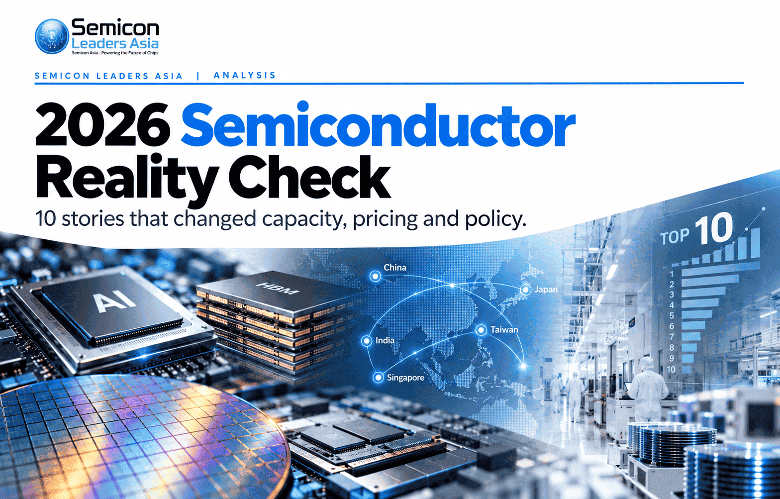
AI chips, HBM, export controls and billion-dollar fabs dominated the headlines. But the developments that actually changed semiconductor capacity, pricing and policy were rarely the loudest ones. They sat one or two layers away from the processor, in memory, packaging, materials and qualification.
Semiconductor headlines in 2026 have been unusually large. AI accelerator demand kept climbing. Memory prices surged. Washington rewrote parts of its China chip policy. Beijing's domestic AI hardware push gathered pace. India committed another ₹1,27,500 crore to semiconductors through Semicon 2.0, and Japan kept putting public and private capital behind Rapidus.
The market numbers make the excitement easy to understand. The Semiconductor Industry Association reported global sales of $403.3 billion in the second quarter alone, up 35.1% on the first quarter. July sales came in at $146.8 billion, and by the end of that month cumulative 2026 sales had already passed the industry's previous highest-ever full-year total. In other words, the industry beat its best year on record with five months still to go.
Growth on that scale tends to flatten analysis. When everything is going up, it becomes tempting to treat every large announcement as equally important, and to assume that the biggest headlines must also be the biggest drivers. That assumption is where most of this year's misreadings began.
A licensing rule can travel around the world in an hour and change very little on the ground. A packaging line expansion or a DRAM allocation decision can barely make the trade press and still determine how many AI servers ship next quarter. Headline size and industry consequence are different things, and 2026 has pulled them further apart than usual.
How we ranked them
Semicon Leaders Asia scored ten of the year's biggest semiconductor stories on two separate measures.
- Headline impact measures how loudly a story travelled: media volume, investor reaction and how often it shaped executive conversation.
- Market consequence asks the harder question: did it materially change capacity, pricing, technology access, supply chains or government policy, and will that change persist into 2027?
- Signal gap is the difference between the two. A positive gap means the story mattered more than the coverage suggested. A negative gap means the attention ran ahead of the substance.
The final ranking weights consequence over noise. The gap column is where the analysis lives: it shows where readers who followed only the headlines would have formed the wrong picture of the year.
|
Rank
|
Story
|
Headline impact
|
Market consequence
|
Gap
|
|
10
|
Overseas fabs move from announcement to execution
|
6/10
|
7/10
|
+1
|
|
9
|
HBM4 becomes the next qualification race
|
8/10
|
6/10
|
-2
|
|
8
|
Chinese semiconductor equipment moves closer to Southeast Asia
|
6/10
|
7/10
|
+1
|
|
7
|
Rapidus gets the money. Now it needs the customers
|
8/10
|
7/10
|
-1
|
|
6
|
Critical minerals become semiconductor policy
|
7/10
|
8/10
|
+1
|
|
5
|
Washington changes the China AI-chip licensing equation
|
10/10
|
7/10
|
-3
|
|
4
|
Huawei's Ascend ramp becomes a volume story
|
9/10
|
8/10
|
-1
|
|
3
|
India moves from fab incentives towards an ecosystem policy
|
8/10
|
9/10
|
+1
|
|
2
|
Advanced packaging becomes the capacity constraint
|
8/10
|
10/10
|
+2
|
|
1
|
AI turns the memory cycle into a supply problem
|
10/10
|
10/10
|
0
|
Two patterns stand out before we go story by story. First, the four stories with negative gaps (US export licensing, HBM4 qualification, Rapidus and Huawei's Ascend) are all about announcements, permissions, milestones and roadmaps. Second, the stories with positive gaps (packaging, materials, India's ecosystem push, overseas execution and Chinese equipment abroad) are about the slower, physical business of building and qualifying capacity. That split is the story of 2026 in miniature.
10. Overseas fabs move from announcement to execution
Headline impact: 6/10 | Market consequence: 7/10 | Signal gap: +1
For several years, geographic diversification in semiconductors was measured mostly in press conferences. Arizona, Kumamoto, Dresden and Singapore each promised a production map that depended less on Taiwan. In 2026 the useful question changed from where fabs were being announced to which of them were turning political commitments into qualified, shipping capacity.
What happened
TSMC remains the clearest test case. Its first Arizona fab has been in high-volume N4 production since late 2024 with yields TSMC describes as good, and on 12 May 2026 its board approved a further capital injection of up to US$20 billion into TSMC Arizona. Construction on a fourth Arizona fab and the company's first US advanced-packaging fab began in early 2026. In Japan, the first Kumamoto fab has been in volume production since the end of 2024, and on 11 August TSMC and Sony Semiconductor Solutions signed a definitive agreement for a new Kumamoto image-sensor venture, with Sony planning about ¥465 billion and TSMC about ¥282 billion. Further out, TSMC's Dresden venture ESMC targets tool-in during 2027, and the VIS-NXP joint venture VSMC is building a US$7.8 billion, 300mm fab in Singapore with production also targeted for 2027.
Why it matters
The detail that matters most in Arizona is not the extra wafer capacity. It is the packaging fab. A leading-edge wafer made in the US but packaged in Taiwan does not give a customer a fully independent supply chain; it simply moves the single point of failure from one step to the next. Pairing fabs with packaging is what turns an overseas site from a political hedge into a credible alternative route for production.
The Sony venture in Kumamoto points to a second shift. Overseas capacity is increasingly being built around a specific anchor customer and product category, rather than as general-purpose leading-edge logic. That is a more commercially durable model, because utilisation is designed in from the start rather than hoped for after the ribbon is cut.
ESMC's own guidance is the reminder of what has not changed. It says its Dresden ramp will depend on customer requirements and market conditions. In plain terms, a fab without committed demand ramps slowly, whatever the subsidy.
What to watch
- Whether US-packaged accelerators begin to be specified separately by hyperscaler customers.
- Cost per wafer disclosures for overseas sites versus Taiwan, which will decide how long customers accept a premium for resilience.
- Customer announcements for ESMC and VSMC ahead of their 2027 start-up dates.
What the market got wrong: geography attracted more attention than utilisation. A fab does not diversify the supply chain when it opens. It does so when qualified wafers ship in meaningful volume and become interchangeable with capacity elsewhere.
9. HBM4 becomes the next qualification race
Headline impact: 8/10 | Market consequence: 6/10 | Signal gap: -2
Every new HBM generation now arrives with something resembling a sporting contest: who samples first, who qualifies with the largest accelerator customer and who claims the highest bandwidth. HBM4 followed the script almost exactly, and the coverage treated each milestone as a potential shift in market share.
What happened
Samsung Electronics said on 12 February that it had begun mass production and commercial shipments of HBM4, built on its 1c DRAM process with a 4nm logic base die. On 16 March, Micron said its 36GB 12-high HBM4 designed for Nvidia's Vera Rubin platform had entered high-volume production, with bandwidth above 2.8TB/s. The same day, SK hynix used Nvidia's GTC 2026 to show HBM4 for Vera Rubin alongside its HBM3E and wider AI-memory portfolio.
Why it matters
The striking fact is not who was first. It is that all three suppliers were in production or commercialisation within roughly five weeks of each other. When every credible supplier clears the same bar at about the same time, qualification stops being the differentiator. Yield, consistency, power characteristics and the ability to deliver contracted volume become the real competition.
That is also why the headline score runs ahead of consequence here. HBM is no longer simply a DRAM product. It sits at the intersection of memory fabrication, through-silicon via processing, stacking, advanced packaging and accelerator design. Samsung's use of a separately manufactured 4nm logic base die shows how far the product has moved towards logic-style manufacturing. A supplier can win a qualification and still lose share if its stacks do not yield at scale or arrive in time for the packaging line.
In a market as undersupplied as 2026, buyers have a strong incentive to qualify every supplier they can, not to pick one winner. That dampens the share swings the headlines kept predicting.
What to watch
- Yield and bit-output commentary on HBM4 in Q4 earnings calls, rather than further qualification announcements.
- How much of each supplier's HBM4 base die is made in-house versus at a foundry, and what that does to cost.
What the market got wrong: HBM4 is not a winner-takes-all qualification contest. With all three suppliers shipping, the deciding question is who can make qualified product at scale without sacrificing yield.
8. Chinese semiconductor equipment moves closer to Southeast Asia
Headline impact: 6/10 | Market consequence: 7/10 | Signal gap: +1
China's equipment push is usually discussed through a single question: how quickly can domestic suppliers replace Applied Materials, Lam Research, KLA, Tokyo Electron and other established toolmakers inside Chinese fabs? A quieter development deserves more attention. Chinese equipment companies are beginning to build commercial relationships in Southeast Asia's expanding manufacturing and packaging base.
What happened
On 30 July, Chinese automated material handling supplier MeetFuture Technology said Southeast Asia was becoming an increasingly important international market for Chinese equipment makers. The company said it had secured AMHS orders from more than ten overseas wafer-fab customers, had set up a global sales centre in Singapore through MFSG, and had opened a manufacturing base and service centre in Malaysia in 2025.
A useful comparison comes from ACM Research, which is headquartered in the US but has substantial operations in China. In February it disclosed delivery of several 300mm single-wafer cleaning systems to a Singapore foundry, its first deployment at a Singapore fab, along with wafer-level advanced-packaging equipment orders from a Singapore-based global OSAT. That is not a Chinese-headquartered example, but it shows how open the region's fabs and OSATs have become to newer equipment suppliers.
Why it matters
Inside China, domestic toolmakers benefit from policy support and from customers who have few alternatives. Outside China, they compete on cost, service and performance against incumbents with decades of installed base. A reference customer in Singapore or Malaysia is therefore worth far more than its order value suggests: it is evidence that the product can win on commercial terms.
It is also telling where the first wins are appearing. Material handling, cleaning and packaging tools are less exposed to export controls and less process-critical than lithography or etch. That is the classic entry route for a challenger: start where qualification is shorter and switching costs are lower, then move up the process flow. Southeast Asia, with its dense OSAT and back-end base, is the natural place to begin.
The near-term effect should not be exaggerated. Established suppliers keep enormous advantages in process knowledge, service networks and qualification history. But competition in equipment changes once a challenger has customers outside its home market, and that threshold has now been crossed in parts of the region.
What to watch
- Whether Chinese suppliers move from handling and cleaning into deposition, etch or metrology at regional fabs.
- How US and allied export policy responds to Chinese tools inside fabs that also serve Western customers.
What the market got wrong: China's equipment challenge is not only about replacing foreign tools inside China. Winning qualification abroad is the harder test, and potentially the more important one.
7. Rapidus gets the money. Now it needs the customers
Headline impact: 8/10 | Market consequence: 7/10 | Signal gap: -1
Japan's Rapidus project has never been short of ambition. In 2026 it also stopped being short of money. What it still lacks is the thing every foundry ultimately lives on: committed production customers.
What happened
On 27 February, Rapidus announced ¥267.6 billion (about US$1.7 billion) of additional funding, including ¥100 billion from Japan's Information-Technology Promotion Agency, as it works towards 2nm mass production in 2027. Reuters reported on 6 October that the company now has roughly US$15 billion of Japanese government backing in total. The same report said Rapidus is working with 17 design partners, including Synopsys and Infosys, but still needs to secure significant manufacturing customers. The company first demonstrated prototype 2nm gate-all-around transistors in July 2025.
Why it matters
Producing working 2nm silicon and running a competitive foundry are different achievements. A foundry needs proven yield, a mature process design kit, a deep IP library, packaging options, reliability data and, above all, customers willing to put a real product on an unproven line. Design partners help build the ecosystem, but they are not the same as wafer orders.
The customer problem is structural. A company choosing a leading-edge foundry is betting a product generation on it. The safe option is the incumbent with the longest yield history. For Rapidus to win, it probably needs either a customer that values a non-Taiwan source enough to accept execution risk, or a niche such as specialised AI or edge chips where its single-wafer processing and short cycle times offer a real advantage.
That makes Rapidus one of the most important experiments in industrial policy anywhere in the industry. It will show whether state capital can shorten the decades it normally takes to build a trusted leading-edge foundry.
What to watch
- A named anchor customer for 2027 production, which would matter more than any further funding round.
- Disclosed yield or defect-density progress on the pilot line.
- Whether Rapidus builds back-end packaging capability alongside the fab, following the same logic as TSMC Arizona.
What the market got wrong: the real question is not whether Japan can finance a 2nm fab. It is whether public money can create a commercially viable leading-edge foundry fast enough to win real production programmes.
6. Critical minerals become semiconductor policy
Headline impact: 7/10 | Market consequence: 8/10 | Signal gap: +1
Semiconductor security used to be discussed in terms of fabs, lithography machines and advanced processors. In 2026 the argument moved upstream, to the materials that feed the entire chain.
What happened
China's licensing controls on rare earths and other strategic materials showed how supply-chain leverage can begin long before a wafer enters a fab. Reuters reported on 13 May that China's exports of controlled heavy rare earths, including yttrium, dysprosium and terbium, remained roughly 50% below earlier levels despite broader diplomatic efforts to ease restrictions.
India moved in the same direction from the other side. The Union Budget 2026-27 announced dedicated Rare Earth Corridors in Odisha, Kerala, Andhra Pradesh and Tamil Nadu. On 1 February the government also announced India Semiconductor Mission 2.0 with an initial ₹1,000 crore provision for FY2026-27, focused on equipment, materials, full-stack Indian IP and supply-chain development, ahead of the full Cabinet approval in July.
Why it matters
The most important lesson from the rare-earth episode is that easing a restriction on paper does not restore supply in practice. Once a licensing system exists, it can be tightened, slowed or applied selectively without a new announcement. Buyers therefore have to plan as if access is conditional, even in periods of diplomatic calm. That changes inventory policy, supplier qualification and long-term contracting across the industry.
Materials exposure is also less visible than tool exposure. A fab knows exactly which lithography machines it depends on. It is much harder to trace which magnets, gases, specialty chemicals or substrates in its supply chain depend on a single country. That opacity is precisely what makes materials such an effective form of leverage, and why governments are now treating minerals policy as part of chip policy rather than as a separate mining question.
What to watch
- Long-term offtake agreements between chipmakers or equipment firms and non-Chinese rare-earth processors.
- How quickly India's rare-earth corridors move from budget line to processing capacity.
What the market got wrong: semiconductor sovereignty cannot be measured by fab capacity alone. Materials, gases, substrates, magnets and equipment components now belong in the same strategic calculation.
5. Washington changes the China AI-chip licensing equation
Headline impact: 10/10 | Market consequence: 7/10 | Signal gap: -3
Few semiconductor policy announcements drew more attention this year. The coverage framed it as Washington reopening the Chinese market to US AI accelerators. The rule itself says something more limited, and more interesting.
What happened
On 13 January, the US Bureau of Industry and Security changed its licence-review policy for certain advanced processors destined for China and Macau, effective 15 January. Products including Nvidia's H200 and AMD's MI325X moved from a presumption of denial to case-by-case review, subject to conditions. Applicants must certify sufficient US supply of the product, show that production for China will not divert relevant global foundry capacity from US customers, meet customer and security controls, and send representative shipments for independent third-party testing in the United States. Aggregate shipments to China and Macau must not exceed 50% of the volume of the same product shipped for US end use.
Why it matters
That last condition is the key to reading the rule. By tying China volumes to US volumes, Washington has not opened a market; it has created a rationing mechanism. China access becomes a function of US demand, foundry allocation and testing capacity, all of which the US government can observe and adjust. Export control has moved from a binary gate to a volume dial.
The commercial effect is also narrower than the headlines suggested. The products covered are not the newest generation, licences are discretionary, and the compliance burden is real. For Chinese buyers, the rule offers access to capable hardware but not certainty of supply. That matters, because uncertainty is exactly what pushes them to keep investing in domestic alternatives, which links this story directly to Huawei's volume ramp below.
This story carries the largest negative signal gap on our list. It dominated attention for weeks, yet its effect on actual chip flows depends on licensing decisions that remain largely out of public view.
What to watch
- Disclosed licence approvals and shipment volumes in Nvidia and AMD filings.
- Whether the 50% cap or the testing requirement is adjusted, which would be the clearest sign of where policy is heading.
What the market got wrong: export policy is no longer an on/off switch. It has become a mechanism for managing which chips, which customers and how much volume can enter China.
4. Huawei's Ascend ramp becomes a volume story
Headline impact: 9/10 | Market consequence: 8/10 | Signal gap: -1
Huawei's AI processors have generated headlines for years, usually in the form of benchmark comparisons with Nvidia. In 2026 the more important question became volume.
What happened
Following the release of DeepSeek V4, Reuters reported on 29 April, citing sources, strong demand for the Ascend 950PR from ByteDance, Tencent, Alibaba and cloud and GPU-service providers, with production of roughly 750,000 units planned for 2026. That figure is source reporting rather than an official Huawei forecast, and Reuters also noted that production continued to face constraints linked to US restrictions on advanced manufacturing equipment.
Huawei's official roadmap put the Ascend 950PR in Q1 2026 and the 950DT in Q4 2026, with the 960 and 970 to follow. At HUAWEI CONNECT 2026 in September, the company said it was moving to a one-generation-a-year cadence, that Ascend 960 development was ahead of its earlier roadmap, and it described a broader UnifiedBus portfolio covering compute, interconnect, storage and system infrastructure.
Why it matters
A domestic accelerator does not need to beat Nvidia's best chip to change China's market. It needs to be available in sufficient volume, at adequate performance, for the workloads Chinese customers actually run. The demand pattern after DeepSeek V4 matters here: efficient Chinese models lower the performance bar that domestic hardware has to clear, which makes volume and software compatibility more important than peak specifications.
The UnifiedBus announcement is arguably as significant as the chip roadmap. Nvidia's lasting advantage has always been the complete system, including interconnect, networking and software, not the processor alone. By building out the same layers, Huawei is trying to compete at the cluster level, where many weaker chips connected efficiently can still deliver useful compute.
The constraint is manufacturing. Without access to the most advanced equipment, Huawei's yields and costs will remain under pressure, and its ramp depends on domestic fabs, domestic HBM and domestic packaging all scaling together. That is also why its progress is a useful indicator for China's wider semiconductor base.
What to watch
- Independent evidence of Ascend shipment volumes, for example through large cluster deployments by Chinese cloud providers.
- Domestic HBM supply for Ascend, which may become a tighter limit than logic capacity.
What the market got wrong: the important contest is not Huawei against Nvidia on peak specifications. It is whether Huawei can reach enough volume to sustain a durable domestic AI-compute ecosystem.
3. India moves from fab incentives towards an ecosystem policy
Headline impact: 8/10 | Market consequence: 9/10 | Signal gap: +1
India's first semiconductor push was dominated by individual projects and the headlines that came with each one. Semicon 2.0 changes the scope of the policy, and arguably the nature of the bet.
What happened
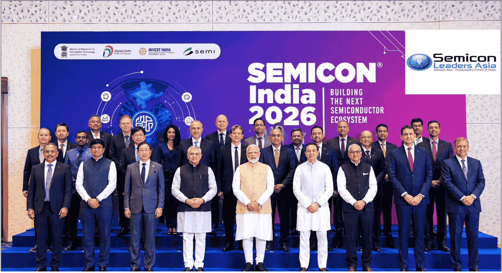
On 15 July, the Union Cabinet approved Semicon 2.0 with a total outlay of ₹1,27,500 crore. Its six pillars cover chip design, semiconductor machines and materials, additional fabs, advanced packaging, research and development, and talent. Under the first programme, India approved 12 semiconductor manufacturing projects across six states, representing more than ₹1.64 lakh crore of committed investment. A Press Information Bureau release dated 19 September said commercial lines at CDIL Semiconductor in Mohali and Suchi Semicon in Surat had taken the number of operational commercial units among those 12 projects to five.
Why it matters
Five operating units is progress, but the more significant change is in what the policy now funds. The first phase attracted anchor projects. It did not, on its own, create the dense web of suppliers that makes those projects competitive: specialty chemicals, gases, equipment service, substrates, design IP, test capability and skilled technicians. Without that web, every fab and OSAT has to import inputs and expertise, which raises costs and slows ramp-up.
Semicon 2.0 is an attempt to fill those gaps. The SEMICON India statement of 19 September identifies equipment, materials, gases, chemicals, precision manufacturing, IP and skilled manpower as part of the wider ecosystem, which is a notably different emphasis from announcement-led industrial policy.
India's realistic near-term opportunity is not leading-edge logic. It is in mature-node, power and compound semiconductors, OSAT and test, and in design, where it already has deep engineering talent. An ecosystem policy suits that position, because those segments compete on cost, reliability and local supply rather than on process leadership. This story carries a positive signal gap because the coverage still tends to measure India against Taiwan, when the more relevant benchmark is Malaysia or Vietnam.
What to watch
- Utilisation and customer wins at the five operating units, particularly export customers.
- The first approvals under the equipment and materials pillar, which will show whether suppliers follow the fabs.
What the market got wrong: India's semiconductor story is not mainly about whether it can challenge Taiwan at the leading edge. The nearer-term test is whether it can turn separate investments into a functioning supply-chain cluster.
2. Advanced packaging becomes the capacity constraint
Headline impact: 8/10 | Market consequence: 10/10 | Signal gap: +2
For decades, the wafer fab received the attention and packaging came afterwards. AI has reversed that hierarchy. In 2026, packaging stopped being the last step in manufacturing and became one of the main limits on how much AI hardware the industry can ship.
What happened
Large accelerators now combine multiple compute dies, HBM stacks, interposers and substrates with increasingly demanding power and thermal designs. TSMC describes its CoWoS platform as a 2.5D technology that integrates compute dies with high-bandwidth memory on an interposer for AI and HPC systems. At its 2026 North America Technology Symposium, TSMC said it was already producing 5.5-reticle CoWoS and planned a 14-reticle version for 2028, able to integrate roughly 10 large compute dies and 20 HBM stacks. On its 16 April Q1 earnings call, CEO C.C. Wei said large-format CoWoS remained the main approach, while a pilot line for the panel-based CoPoS was being built for later production. In August, TSMC's board approved capital spending for installing and upgrading advanced-packaging capacity alongside wafer capacity.
Why it matters
The arithmetic of AI hardware has changed. An extra leading-edge wafer is useful only if it can be packaged with HBM into a working system. If packaging capacity lags wafer capacity, the wafers wait. That makes packaging the effective governor on AI supply, and gives whoever controls it considerable pricing and allocation power.
A move from 5.5 to 14 reticles in two years is not an incremental step. It means a single package containing several times as much silicon and memory, which in turn demands larger and flatter substrates, more precise bonding, better thermal solutions and package-aware design tools. As our earlier chiplet analysis argued, packaging is becoming part of the chip architecture itself.
The consequences run across the whole supply chain. OSATs need new equipment. Substrate suppliers need new materials and formats. HBM makers need tighter stacking. EDA vendors need design flows that treat the package as part of the system. And customers now have to reserve packaging capacity at the same time as wafers, which changes procurement from a single negotiation into a coordinated one.
What to watch
- CoWoS capacity additions versus accelerator demand in TSMC's Q4 guidance.
- Qualification of OSATs outside TSMC for large-format 2.5D packaging, which would ease the bottleneck.
- Substrate supply for very large packages, a likely next pinch point.
What the market got wrong: the AI chip shortage was often described as a shortage of leading-edge silicon. Increasingly, the scarce resource is the ability to turn that silicon and HBM into one qualified package.
1. AI turns the memory cycle into a supply problem
Headline impact: 10/10 | Market consequence: 10/10 | Signal gap: 0
The biggest semiconductor story of 2026 is not another GPU. It is what AI has done to memory. This is the only story on our list where the headlines and the consequences were equally large, and the consequences are still spreading.
What happened
HBM attracts the attention because it sits beside the accelerator. But the effects have spread into the wider DRAM market as suppliers shift capital, cleanroom space and wafers towards higher-value AI products. On 30 July, Samsung said its memory business had delivered record quarterly revenue and operating profit while serving AI demand with limited capacity, and that it expected the memory market to remain undersupplied, with server DRAM, enterprise SSD and HBM demand accelerating in the second half. Reuters reported on 6 October that TrendForce expected conventional DRAM prices to rise 10 to 15% quarter on quarter in Q3, after an increase of roughly 60% in Q2.
Micron went further. Reporting fiscal Q4 and FY2026 results on 30 September, CEO Sanjay Mehrotra said demand was expected to exceed supply through 2027 and 2028, with no clear line of sight to when the market would return to balance. Micron has pointed to cleanroom constraints and the higher wafer trade ratio of HBM as the main limits on supply growth, and has raised capital spending in response.
Why it matters
The mechanism is what makes this story structural rather than cyclical. HBM uses far more wafer area per bit than conventional DRAM. Every wafer moved to HBM to serve AI therefore removes a larger amount of conventional DRAM supply than it adds in HBM. AI is not just adding demand to the memory market; it is subtracting supply from the rest of it.
That explains why prices for ordinary DRAM, used in PCs, phones, servers and cars, rose so sharply in a year when much of that end demand was unremarkable. It also explains why the shortage is hard to fix quickly. New capacity requires new cleanroom space, which takes years to build, and suppliers have every reason to keep prioritising higher-margin AI products when that space arrives.
Memory has historically been the most cyclical part of the industry, with booms reliably followed by gluts. A supplier saying publicly that tightness may last through 2028 is therefore unusual. If it proves right, memory makers will have more pricing power for longer than in any previous cycle, and device makers outside AI will face a sustained cost squeeze.
What to watch
- Q4 contract pricing for conventional DRAM and NAND, and whether the rate of increase slows.
- Cleanroom completion dates at Samsung, SK hynix and Micron, which set the real ceiling on 2027 supply.
- Margin pressure and pricing moves among PC, smartphone and automotive makers.
What the market got wrong: investors initially treated AI as a logic-chip supercycle. In 2026 it became clear that it is a system-wide capacity cycle, with memory and packaging increasingly deciding how much AI compute can actually ship.
The Semicon Leaders Asia view
The striking thing about 2026 is not simply that semiconductor demand grew. It is where the industry's constraints moved.
The biggest headlines were usually about processors: Nvidia products, Huawei accelerators, 2nm technology and export controls. The developments with the greatest consequences were often one or two layers away from the processor: HBM availability, CoWoS capacity, materials, equipment qualification and the design of government incentives. Read across all ten stories, three themes stand out.
1. The bottleneck has moved away from the logic wafer
Memory and packaging, our top two stories, both describe the same shift. AI demand is pulling on every part of the system, and the slowest-moving parts now set the pace. For buyers, that means securing memory and packaging allocations is as strategic as securing wafers. For investors, it means value is accruing to parts of the chain that were long treated as commodities.
2. Policy has become a tool for managing flows, not just blocking them
The US licensing rule, China's minerals licensing and India's Semicon 2.0 look very different, but they share a logic. Governments are moving from simple bans and grants towards instruments that control volume, direction and the shape of supply chains over time. That makes policy risk more continuous and less predictable, and harder to capture in a single headline.
3. Execution is now the scarce asset
Rapidus has funding but needs customers. Overseas fabs have buildings but need utilisation. HBM4 suppliers have qualifications but need yield. Chinese equipment makers have products but need foreign reference customers. In each case, the announcement is the easy part and the commercial proof is the hard part.
That matters particularly for Asia, where almost every one of these stories is located. Taiwan still anchors leading-edge foundry and advanced packaging. South Korea sits at the centre of the HBM race, with Samsung and SK hynix both shipping HBM4 alongside Micron. Japan is attempting to rebuild leading-edge logic through Rapidus while keeping its deep strength in materials and equipment. China is pushing domestic accelerators and tools further into commercial use, at home and now in Southeast Asia. India has widened its policy from attracting individual plants to building an entire ecosystem. Singapore and Malaysia are becoming the meeting point for suppliers from all of them.
The geography is changing, but not in the simple way the phrase "supply-chain diversification" suggests. New fabs do not immediately replace established clusters. New AI chips do not immediately replace Nvidia. A qualification announcement does not guarantee HBM volume. And government funding does not guarantee a commercially successful foundry.
Capacity that ships matters more than capacity that is announced. That may be the clearest lesson from semiconductor markets in 2026 so far.
The industry entered the year asking which company would build the fastest AI chip. It is ending it with harder questions: who can supply the memory, package the silicon, secure the materials, qualify the equipment and finance the fabs needed to make those chips at scale. The companies and countries with good answers to those questions, rather than the loudest announcements, are the ones likely to define 2027.
Sources
Semiconductor Industry Association (6 August and 4 September 2026); US Bureau of Industry and Security and Federal Register final rule (13 and 15 January 2026); Press Information Bureau, Government of India (1 February, 15 July, 17 and 19 September 2026); TSMC (Q1 earnings call 16 April, North America Technology Symposium, board resolutions of 12 May and August 2026, Sony venture announcement 11 August 2026); ESMC; VSMC; Samsung Electronics (12 February and 30 July 2026); SK hynix Newsroom (16 March 2026); Micron Technology (16 March and 30 September 2026); Rapidus (27 February 2026); Huawei (HUAWEI CONNECT 2026); MeetFuture Technology (30 July 2026); ACM Research (26 February 2026); Reuters (29 April, 13 May and 6 October 2026), including TrendForce estimates; The Wall Street Journal (30 September 2026).